- 您现在的位置:买卖IC网 > PDF目录2159 > MAX9937AXK+T (Maxim Integrated Products)IC AMP CURRENT SENSE SC70-5 PDF资料下载
参数资料
| 型号: | MAX9937AXK+T |
| 厂商: | Maxim Integrated Products |
| 文件页数: | 10/11页 |
| 文件大小: | 0K |
| 描述: | IC AMP CURRENT SENSE SC70-5 |
| 产品培训模块: | Lead (SnPb) Finish for COTS Obsolescence Mitigation Program |
| 标准包装: | 1 |
| 放大器类型: | 电流检测 |
| 电路数: | 1 |
| -3db带宽: | 350kHz |
| 电流 - 输入偏压: | 2µA |
| 电压 - 输入偏移: | 300µV |
| 电流 - 电源: | 20µA |
| 电流 - 输出 / 通道: | 22mA |
| 电压 - 电源,单路/双路(±): | 2.7 V ~ 5.5 V |
| 工作温度: | -40°C ~ 125°C |
| 安装类型: | 表面贴装 |
| 封装/外壳: | 6-TSSOP(5 引线),SC-88A,SOT-353 |
| 供应商设备封装: | SC-70-5 |
| 包装: | 标准包装 |
| 产品目录页面: | 1392 (CN2011-ZH PDF) |
| 其它名称: | MAX9937AXK+TDKR |
MAX9937
Detailed Description
The MAX9937 unidirectional high-side, current-sense
amplifier features a 4V to 28V input common-mode volt-
age range that is independent of supply voltage (VCC =
2.7V to 5.5V). The MAX9937 monitors the current through
a current-sense resistor by converting the sense voltage
to a current output (OUT). Gain is set by the ratio of an
output resistor (ROUT) and an input resistor (RRSP). High-
side current monitoring with the MAX9937 does not inter-
fere with the ground path of the load, making it useful for
a variety of automotive battery/ECU monitoring.
Robust input ESD structure allows input common-mode
voltages to exceed the 28V maximum operating input
range for short durations, making the MAX9937 ideal
for applications that need to withstand short-duration
load-dump conditions. The MAX9937 is able to with-
stand reverse-battery conditions by a suitable choice of
input resistors (RRSN, RRSP). See the Input Common-
Mode Voltages > 28V and < 0V section.
Current-Sense Amplifier Operation
The MAX9937 current-sense amplifier operation is best
understood as a specialized op-amp circuit with a
p-channel FET in the feedback path. The op amp
forces a current through an external gain resistor at
RSP (RRSP, see the Typical Application Circuit) so that
its voltage drop equals the voltage drop across the
external sense resistor, RSENSE, making the voltage at
RSP the same as RSN. An external resistor at RSN
(RRSN) has the same value as RRSP to minimize input
offset voltage due to input bias currents.
The current through RRSP is now sourced by the high-
voltage p-channel FET into an external resistor (ROUT)
at OUT. This produces an output voltage whose magni-
tude is given by the following equations:
The gain accuracy is primarily determined by the
matching of the two gain resistors, RRSP and ROUT. The
voltage gain error of the MAX9937 is less than 1.5%.
Total gain = 20V/V with ROUT = 10kΩ
and RRSP = 500Ω.
Low temperature drift of input bias currents and input
offset currents minimizes their impact on total input off-
set voltage of the current-sense amplifier.
Applications Information
Choosing RSENSE
To measure lower currents more accurately, use a high
value for RSENSE. The high value develops a higher
sense voltage that reduces the effect of offset voltage
errors of the internal op amp. In applications monitoring
very high currents, however, RSENSE must be able to
dissipate the I2R losses. If the resistor’s rated power
dissipation is exceeded, its value may drift or it may fail
altogether, causing large differential voltages to devel-
op between RSP and RSN.
To minimize the effect of input offset voltage by produc-
tion calibration, see the
Skewed Input Offset Voltage for
Production Calibration section. This can help reduce
the size of the sense resistor in high-current applica-
tions, as well as measure wide-dynamic-range currents
without sacrificing accuracy.
If ISENSE has a large high-frequency component, mini-
mize the inductance of RSENSE and use input differen-
tial filters (see the
Flexible EMI Filtering section).
Low-inductance metal-film resistors are best suited for
these applications.
Calculation of Total Input Offset Voltage
Because of the use of op-amp style architecture, calcu-
lation of total input offset voltage involves the same
methodology as is used for any standard op-amp cir-
cuit. Interaction of the input bias currents and tolerance
of the external resistors, combined with the core input
offset voltage of the op amp, are important to consider.
Finally, RSS (root-sum-of-squares) calculation for all
these uncorrelated sources of error gives the final input
offset voltage.
()
(
)
(
)
(
)
VV
I
R
I
R
OS FINAL
OS
B
RS
B
RS
=+
×
+
×
22
2
ΔΔ
VI
R
VV
R
SENSE
LOAD
SENSE
OUT
SENSE
OUT
RSP
=×
Automotive Current-Sense Amplifier
with Reverse-Battery Protection
8
_______________________________________________________________________________________
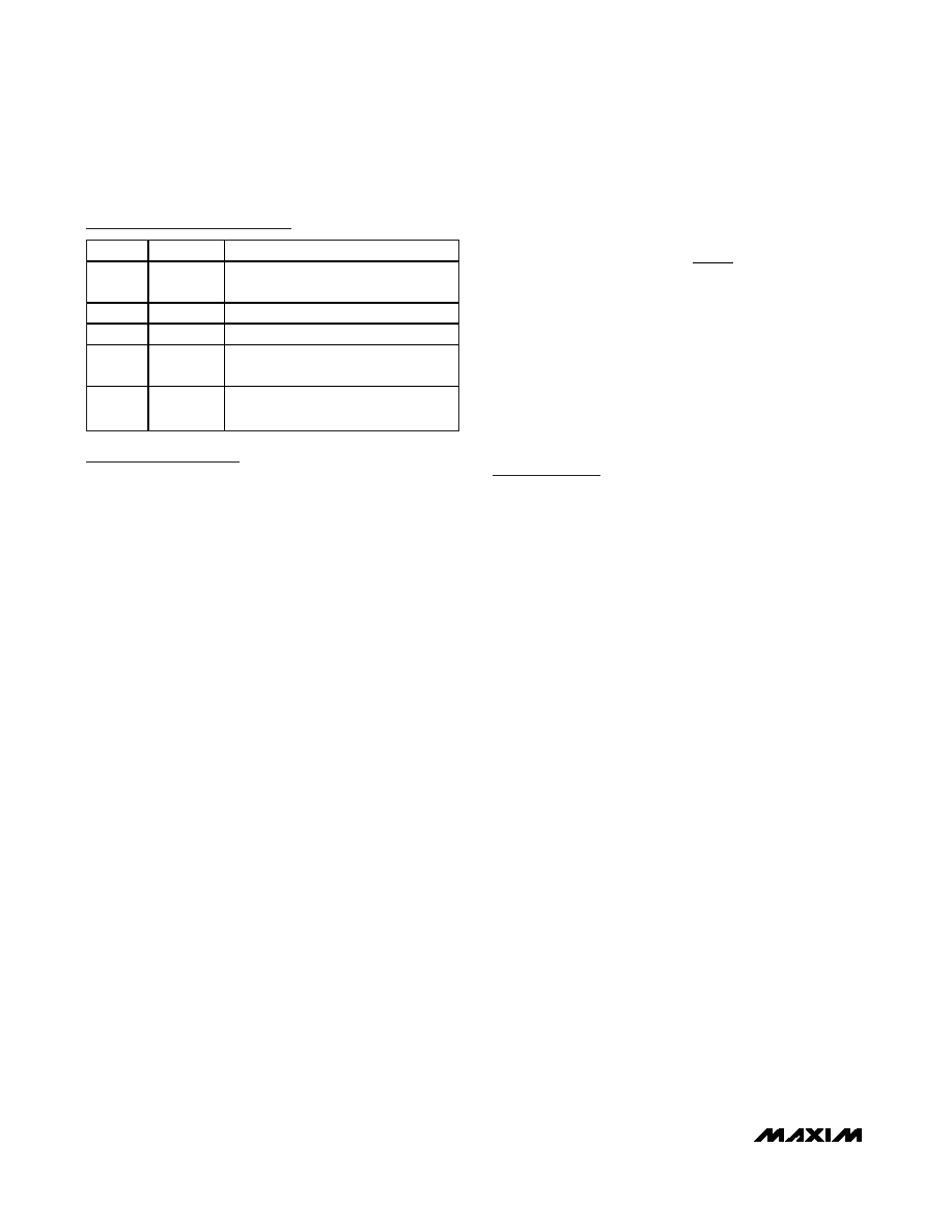
Pin Description
PIN
NAME
FUNCTION
1VCC
Power Supply. Bypass to GND with a
0.1F capacitor.
2
GND
Ground
3
OUT
Current Output
4
RSN
Load-Side Connection Through
External RRSN Resistor
5
RSP
Supply-Side Connection Through
External RRSP Resistor
相关PDF资料 |
PDF描述 |
|---|---|
| MAX9938WEUK+T | IC AMP CURRENT SENSE SOT23-5 |
| MAX9939AUB+T | IC AMP PGA SPI VOS I/O 10MSOP |
| MAX9943AUA+T | IC OPAMP PREC LP/HV SGL 8-MSOP |
| MAX9945AUA+T | IC OPAMP MOS-INPUT LP/LN 8-MSOP |
| MC33077P | IC OPAMP DUAL LOW NOISE 8DIP |
相关代理商/技术参数 |
参数描述 |
|---|---|
| MAX9937EVKIT+ | 功能描述:放大器 IC 开发工具 MAX9937 Eval Kit RoHS:否 制造商:International Rectifier 产品:Demonstration Boards 类型:Power Amplifiers 工具用于评估:IR4302 工作电源电压:13 V to 23 V |
| MAX9938EVKIT+ | 功能描述:放大器 IC 开发工具 MAX9938 Eval Kit RoHS:否 制造商:International Rectifier 产品:Demonstration Boards 类型:Power Amplifiers 工具用于评估:IR4302 工作电源电压:13 V to 23 V |
| MAX9938FEBS+G45 | 制造商:Maxim Integrated Products 功能描述:1?A, 4-BUMP UCSP/SOT23,PRECISION CURRENT-SENSE AMPLIFIER - Rail/Tube |
| MAX9938FEBS+T | 功能描述:电流灵敏放大器 1uA Bump Precision Current Sense Amp RoHS:否 制造商:Texas Instruments 通道数量: 共模抑制比(最小值):110 dB 输入补偿电压:80 uV 电源电压-最大:5.5 V 电源电压-最小:2.7 V 电源电流:350 uA 最大工作温度:+ 125 C 最小工作温度:- 40 C 安装风格:SMD/SMT 封装 / 箱体:VQFN-16 封装:Reel |
| MAX9938FEBS+TG45 | 功能描述:电流灵敏放大器 1uA Bump Precision Current Sense Amp RoHS:否 制造商:Texas Instruments 通道数量: 共模抑制比(最小值):110 dB 输入补偿电压:80 uV 电源电压-最大:5.5 V 电源电压-最小:2.7 V 电源电流:350 uA 最大工作温度:+ 125 C 最小工作温度:- 40 C 安装风格:SMD/SMT 封装 / 箱体:VQFN-16 封装:Reel |
发布紧急采购,3分钟左右您将得到回复。