- 您现在的位置:买卖IC网 > PDF目录2159 > MAX9937AXK+T (Maxim Integrated Products)IC AMP CURRENT SENSE SC70-5 PDF资料下载
参数资料
| 型号: | MAX9937AXK+T |
| 厂商: | Maxim Integrated Products |
| 文件页数: | 4/11页 |
| 文件大小: | 0K |
| 描述: | IC AMP CURRENT SENSE SC70-5 |
| 产品培训模块: | Lead (SnPb) Finish for COTS Obsolescence Mitigation Program |
| 标准包装: | 1 |
| 放大器类型: | 电流检测 |
| 电路数: | 1 |
| -3db带宽: | 350kHz |
| 电流 - 输入偏压: | 2µA |
| 电压 - 输入偏移: | 300µV |
| 电流 - 电源: | 20µA |
| 电流 - 输出 / 通道: | 22mA |
| 电压 - 电源,单路/双路(±): | 2.7 V ~ 5.5 V |
| 工作温度: | -40°C ~ 125°C |
| 安装类型: | 表面贴装 |
| 封装/外壳: | 6-TSSOP(5 引线),SC-88A,SOT-353 |
| 供应商设备封装: | SC-70-5 |
| 包装: | 标准包装 |
| 产品目录页面: | 1392 (CN2011-ZH PDF) |
| 其它名称: | MAX9937AXK+TDKR |
MAX9937
Automotive Current-Sense Amplifier
with Reverse-Battery Protection
2
_______________________________________________________________________________________
ABSOLUTE MAXIMUM RATINGS
ELECTRICAL CHARACTERISTICS
(VCC = 5V, VBAT = VRS+ = 12V, VSENSE = (VRS+ - VRS-) = 0, RRSP = RRSN = 500Ω, ROUT = 10kΩ, TA = -40°C to +125°C. Typical
values are at TA = +25°C, unless otherwise noted. See the Typical Application Circuit.) (Note 2)
Stresses beyond those listed under “Absolute Maximum Ratings” may cause permanent damage to the device. These are stress ratings only, and functional
operation of the device at these or any other conditions beyond those indicated in the operational sections of the specifications is not implied. Exposure to
absolute maximum rating conditions for extended periods may affect device reliability.
RSP, RSN to GND Voltage Continuous ..................-0.3V to +30V
RSP, RSN to GND Load-Dump Voltage Duration
(VBAT = 40V) with Typical Application Circuit .......................1s
RSP, RSN to GND Reverse-Battery Voltage Duration
(VBAT = -20V) with Typical Application Circuit........Continuous
Differential Input Voltage (RSP - RSN)................................±0.3V
VCC to GND ...........................................................-0.3V to +6.0V
OUT to GND ...............................................-0.3V to (VCC + 0.3V)
Output Short Circuit to Ground ..................................Continuous
Continuous Input Current into RSN, RSP* ........................±50mA
Continuous Input Current into OUT*.................................±25mA
Thermal Limits (Note 1)
5 SC70 Multiple-Layer PCB
Continuous Power Dissipation (TA = +70°C)
(derate 3.1mW/°C above +70°C) ............................246.9mW
θJA...............................................................................324°C/W
θJC...............................................................................115°C/W
Operating Temperature Range .........................-40°C to +125°C
Junction Temperature ......................................................+150°C
Lead Temperature (soldering, 10s) .................................+300°C
Lead Temperature (reflow) ..............................................+260°C
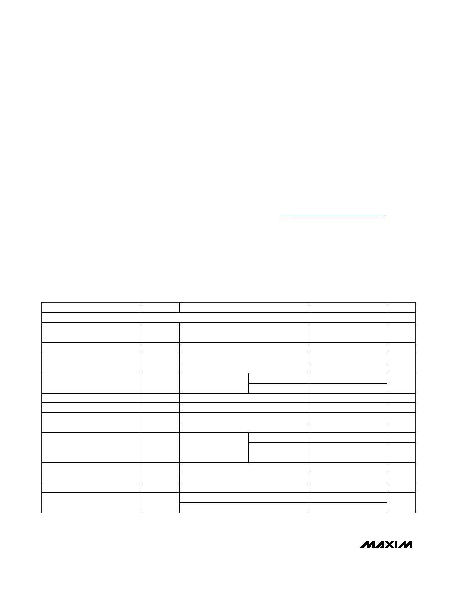
PARAMETER
SYMBOL
CONDITIONS
MIN
TYP
MAX
UNITS
DC CHARACTERISTICS
Input Common-Mode Voltage
Range
VRSP,
VRSN
Inferred from CMRR test
4
28
V
Supply Voltage Range
VCC
Inferred from PSRR test
2.7
5.5
V
TA = +25°C
±0.3
±1.2
Input Offset Voltage (Note 3)
VOS
TA = -40°C to +125°C
±1.6
mV
TA = +25°C
100
120
Common-Mode Rejection Ratio
CMRR
VBAT = +4V to +28V
TA = +125°C
90
dB
Power-Supply Rejection Ratio
PSRR
VCC = +2.7V to +5.5V
90
120
dB
Quiescent Supply Current
ICC
VCC = 5V
20
55
A
TA = +25°C
0.8
2
5.6
Input Bias Current (Note 4)
IB+, IB-
TA = -40°C to +125°C
0.65
6.5
A
TA = +25°C
±1
±12
%
Input Bias Current Mismatch
ΔIB / IB
2 x (IB+ - IB-)/(IB++IB-)
TA = -40°C to
+125°C
±15
%
TA = +25°C, VCC = 0
0.01
1
Input Current in Shutdown
IRSP + IRSN
TA = -40°C to +125°C, VCC = 0
10
A
Voltage Gain
Gain = ROUT/RRSP
20
V/V
TA = +25°C
±0.2
±1.5
Voltage Gain Error (Notes 3, 5)
TA = -40°C to +125°C
±2.0
%
Note 1: Package thermal resistances were obtained using the method described in JEDEC specification JESD51-7, using a 4-layer
board. For detailed information on package thermal considerations, refer to www.maxim-ic.com/thermal-tutorial.
*
Junction temperature rating due to power dissipation must also be observed.
相关PDF资料 |
PDF描述 |
|---|---|
| MAX9938WEUK+T | IC AMP CURRENT SENSE SOT23-5 |
| MAX9939AUB+T | IC AMP PGA SPI VOS I/O 10MSOP |
| MAX9943AUA+T | IC OPAMP PREC LP/HV SGL 8-MSOP |
| MAX9945AUA+T | IC OPAMP MOS-INPUT LP/LN 8-MSOP |
| MC33077P | IC OPAMP DUAL LOW NOISE 8DIP |
相关代理商/技术参数 |
参数描述 |
|---|---|
| MAX9937EVKIT+ | 功能描述:放大器 IC 开发工具 MAX9937 Eval Kit RoHS:否 制造商:International Rectifier 产品:Demonstration Boards 类型:Power Amplifiers 工具用于评估:IR4302 工作电源电压:13 V to 23 V |
| MAX9938EVKIT+ | 功能描述:放大器 IC 开发工具 MAX9938 Eval Kit RoHS:否 制造商:International Rectifier 产品:Demonstration Boards 类型:Power Amplifiers 工具用于评估:IR4302 工作电源电压:13 V to 23 V |
| MAX9938FEBS+G45 | 制造商:Maxim Integrated Products 功能描述:1?A, 4-BUMP UCSP/SOT23,PRECISION CURRENT-SENSE AMPLIFIER - Rail/Tube |
| MAX9938FEBS+T | 功能描述:电流灵敏放大器 1uA Bump Precision Current Sense Amp RoHS:否 制造商:Texas Instruments 通道数量: 共模抑制比(最小值):110 dB 输入补偿电压:80 uV 电源电压-最大:5.5 V 电源电压-最小:2.7 V 电源电流:350 uA 最大工作温度:+ 125 C 最小工作温度:- 40 C 安装风格:SMD/SMT 封装 / 箱体:VQFN-16 封装:Reel |
| MAX9938FEBS+TG45 | 功能描述:电流灵敏放大器 1uA Bump Precision Current Sense Amp RoHS:否 制造商:Texas Instruments 通道数量: 共模抑制比(最小值):110 dB 输入补偿电压:80 uV 电源电压-最大:5.5 V 电源电压-最小:2.7 V 电源电流:350 uA 最大工作温度:+ 125 C 最小工作温度:- 40 C 安装风格:SMD/SMT 封装 / 箱体:VQFN-16 封装:Reel |
发布紧急采购,3分钟左右您将得到回复。