- 您现在的位置:买卖IC网 > Datasheet目录475 > MAX9989ETP+T (Maxim Integrated)IC BUFFER LO 20-TQFN Datasheet资料下载
参数资料
| 型号: | MAX9989ETP+T |
| 厂商: | Maxim Integrated |
| 文件页数: | 8/12页 |
| 文件大小: | 0K |
| 描述: | IC BUFFER LO 20-TQFN |
| 产品培训模块: | Lead (SnPb) Finish for COTS Obsolescence Mitigation Program |
| 标准包装: | 2,500 |
| 功能: | LO 缓冲器/分路器 |
| 频率: | 700MHz ~ 1.1GHz |
| RF 型: | 手机,GSM,DCS,PCS,UMTS |
| 次要属性: | 40dB 反向隔离 |
| 封装/外壳: | 20-WQFN 裸露焊盘 |
| 包装: | 带卷 (TR) |
�� �
�
�+14dBm� to� +20dBm� LO� Buffers�
�with� ±1dB� Variation�
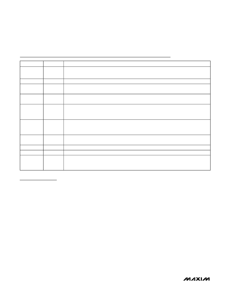
�Pin� Description�
�PIN�
�1,� 4,� 8,� 9,�
�13� –� 18,� EP�
�2�
�3�
�5�
�6�
�7�
�10�
�11,� 12�
�19�
�20�
�NAME�
�GND�
�IN�
�VCCREF�
�REF�
�BIASIN�
�BIASOUT�
�OUTLO�
�VCC2�
�VCC1�
�OUTPLL�
�FUNCTION�
�Ground.� Provide� 5� –� 10� plated� vias� from� EP� to� system� ground� plane� for� optimal� thermal� and� RF�
�performance.�
�Input.� Internally� matched� 50� ?� RF� input.� AC� couple� to� this� pin� so� as� not� to� disturb� input� bias� level.�
�Supply.� Supply� connection� for� on-chip� voltage� and� current� references.� See� Applications� Information�
�for� information� on� decoupling.�
�Voltage� Reference� Output.� Output� for� on-chip� 1.5V� bandgap� voltage� reference.� See� the�
�Applications� Information� section� for� information� on� decoupling.�
�Bias� Connection� for� Input� Buffer.� Set� compressed� power� point� for� input� amplifier� with� a� resistor� to�
�REF� or� GND.� For� +17dBm� output� power,� no� external� biasing� resistors� are� required.� See� the�
�Applications� Information� section� for� more� information.�
�Bias� Connection� for� LO� Output� Amplifier.� Set� compressed� power� point� for� OUTLO� with� a� resistor� to�
�REF� or� ground.� For� +17dBm� output� power,� no� external� biasing� resistors� are� required.� See� the�
�Applications� Information� section� for� more� information.�
�LO� Output.� Internally� matched� 50� ?� RF� output.� AC� couple� to� this� pin� so� as� not� to� disturb� output� bias�
�level.�
�Supply.� Supply� connection� for� OUTLO.�
�Supply.� Supply� connection� for� input� amplifier.�
�PLL� Output.� Output� for� driving� optional� external� PLL.� Requires� external� 100� ?� pullup� to� V� CC� for� bias.�
�For� applications� not� requiring� the� PLL� driver,� removing� R1� leaves� OUTPLL� unbiased,� saving� about�
�12mA� current.�
�Detailed� Description�
�The� MAX9989/MAX9990� LO� buffers� each� consist� of� a�
�single-input� amplifier,� an� output� amplifier,� and� a� second�
�buffer� amplifier� to� drive� the� LO� ’� s� PLL.� The� bias� currents�
�for� the� amplifiers� are� adjustable� through� off-chip� resis-�
�tors,� allowing� the� output� level� to� be� precision� set� any-�
�where� from� +14dBm� to� +20dBm.� The� PLL� output� is�
�preset� to� +3dBm� (about� 900mV� P-P� into� 50� ?� ).�
�Power� levels� are� typically� ±1dB� over� the� full� supply,� input�
�power,� and� temperature� range.� Precision� power� control�
�is� achieved� by� internal� control� circuitry.� Maintaining� tight�
�power� control� keeps� the� system� engineer� from� over�
�specifying� the� LO� drive� in� order� to� guarantee� a� linearity�
�specification� in� the� base-station� mixer.� More� than� 40dB�
�isolation� between� the� LO� output� and� the� input� prevents�
�VCO� pulling.�
�The� MAX9989� is� specified� from� 700MHz� to� 1100MHz,�
�and� the� MAX9990� is� specified� from� 1500MHz� to�
�2200MHz.� Both� are� offered� in� compact� 5mm� ?� 5mm� 20-�
�pin� QFN� thin� packages� with� EP.�
�Input� Amplifier�
�A� single� low-noise� input� amplifier� provides� gain� and� iso-�
�lation.� The� compressed� output� power� for� this� stage� is�
�controlled� by� the� bias� setting� resistors� R2� or� R4� (see� the�
�Typical� Application� Circuit� ).� These� resistors� are� not�
�required� for� the� nominal� +17dBm� output;� see� Table� 1� for�
�bias� resistor� values� to� obtain� +14dBm� to� +20dBm� out-�
�put� power.�
�The� input� is� internally� matched� to� 50� ?� ,� and� typical�
�VSWR� is� no� more� than� 2:1� over� all� operating� conditions.�
�Since� the� input� is� internally� biased,� provide� a� DC� block�
�at� the� input� pin.�
�PLL� Amplifier� and� Output�
�A� small� amount� of� power� is� tapped� off� from� the� input�
�amplifier� ’� s� output,� and� fed� to� a� high-isolation� buffer� to�
�drive� the� PLL� output� at� about� +3dBm.� If� the� PLL� output�
�is� not� required,� it� can� be� disabled� by� removing� R1;� dis-�
�abling� the� PLL� output� saves� 12mA� supply� current.�
�8�
�_______________________________________________________________________________________�
�相关PDF资料 |
PDF描述 |
|---|---|
| MAX9990EVKIT | EVAL KIT FOR MAX9990 |
| MAX9993ETP+D | IC MIXER DOWN CONV 20-TQFN |
| MAX9993EVKIT | EVAL KIT FOR MAX9993 |
| MAX9994ETP+T | IC MIXER DOWN CONV 20-TQFN |
| MAX9994EVKIT | EVAL KIT FOR MAX9994 |
相关代理商/技术参数 |
参数描述 |
|---|---|
| MAX9989EVKIT | 功能描述:射频开发工具 RoHS:否 制造商:Taiyo Yuden 产品:Wireless Modules 类型:Wireless Audio 工具用于评估:WYSAAVDX7 频率: 工作电源电压:3.4 V to 5.5 V |
| MAX998ESA | 功能描述:校验器 IC Single Low Power Comparator RoHS:否 制造商:STMicroelectronics 产品: 比较器类型: 通道数量: 输出类型:Push-Pull 电源电压-最大:5.5 V 电源电压-最小:1.1 V 补偿电压(最大值):6 mV 电源电流(最大值):1350 nA 响应时间: 最大工作温度:+ 125 C 安装风格:SMD/SMT 封装 / 箱体:SC-70-5 封装:Reel |
| MAX998ESA+ | 功能描述:校验器 IC Single Low Power Comparator RoHS:否 制造商:STMicroelectronics 产品: 比较器类型: 通道数量: 输出类型:Push-Pull 电源电压-最大:5.5 V 电源电压-最小:1.1 V 补偿电压(最大值):6 mV 电源电流(最大值):1350 nA 响应时间: 最大工作温度:+ 125 C 安装风格:SMD/SMT 封装 / 箱体:SC-70-5 封装:Reel |
| MAX998ESA+T | 功能描述:校验器 IC Single Low Power Comparator RoHS:否 制造商:STMicroelectronics 产品: 比较器类型: 通道数量: 输出类型:Push-Pull 电源电压-最大:5.5 V 电源电压-最小:1.1 V 补偿电压(最大值):6 mV 电源电流(最大值):1350 nA 响应时间: 最大工作温度:+ 125 C 安装风格:SMD/SMT 封装 / 箱体:SC-70-5 封装:Reel |
| MAX998ESA-T | 功能描述:校验器 IC Single Low Power Comparator RoHS:否 制造商:STMicroelectronics 产品: 比较器类型: 通道数量: 输出类型:Push-Pull 电源电压-最大:5.5 V 电源电压-最小:1.1 V 补偿电压(最大值):6 mV 电源电流(最大值):1350 nA 响应时间: 最大工作温度:+ 125 C 安装风格:SMD/SMT 封装 / 箱体:SC-70-5 封装:Reel |
发布紧急采购,3分钟左右您将得到回复。