- 您现在的位置:买卖IC网 > PDF目录1946 > MAXQ2010-RFX+ (Maxim Integrated Products)IC MCU 16BIT 64KB FLASH 100-LQFP PDF资料下载
参数资料
| 型号: | MAXQ2010-RFX+ |
| 厂商: | Maxim Integrated Products |
| 文件页数: | 11/34页 |
| 文件大小: | 0K |
| 描述: | IC MCU 16BIT 64KB FLASH 100-LQFP |
| 产品培训模块: | Lead (SnPb) Finish for COTS Obsolescence Mitigation Program |
| 标准包装: | 1 |
| 系列: | MAXQ® |
| 核心处理器: | RISC |
| 芯体尺寸: | 16-位 |
| 速度: | 10MHz |
| 连通性: | I²C,SPI,UART/USART |
| 外围设备: | 欠压检测/复位,LCD,POR,PWM,WDT |
| 输入/输出数: | 55 |
| 程序存储器容量: | 64KB(32K x 16) |
| 程序存储器类型: | 闪存 |
| RAM 容量: | 2K x 8 |
| 电压 - 电源 (Vcc/Vdd): | 2.7 V ~ 3.6 V |
| 数据转换器: | A/D 8x12b |
| 振荡器型: | 内部 |
| 工作温度: | -40°C ~ 85°C |
| 封装/外壳: | 100-LQFP |
| 包装: | 托盘 |
第1页第2页第3页第4页第5页第6页第7页第8页第9页第10页当前第11页第12页第13页第14页第15页第16页第17页第18页第19页第20页第21页第22页第23页第24页第25页第26页第27页第28页第29页第30页第31页第32页第33页第34页
MAXQ2010
16-Bit Mixed-Signal Microcontroller
with LCD Interface
______________________________________________________________________________________
19
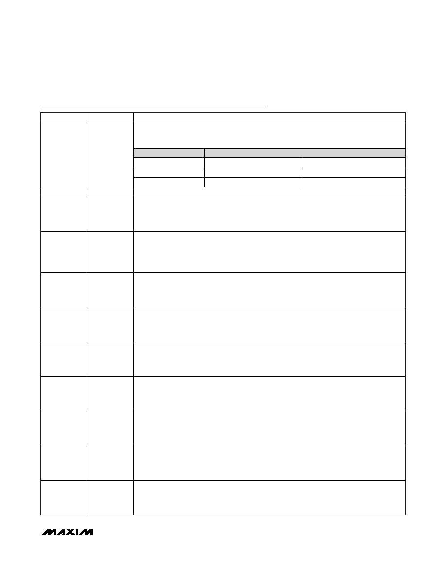
Pin Description (continued)
PIN
NAME
FUNCTION
LCD Segment-Driver Output; LCD Common Drive Output. These pins function as LCD
segment or common drive outputs. Configuring a pin as a common drive output disables the
segment function for that pin.
PIN
SPECIAL/ALTERNATE FUNCTION
10
COM3
SEG40
9
COM2
SEG41
10, 9, 8
COM3, COM2,
COM1; SEG40,
SEG41, SEG42
8
COM1
SEG42
7COM0
LCD Common Drive 0, Output. This pin functions as a LCD common-drive output.
68
P5.0/INT8/
TB0B/RX0
Digital I/O, Type D Port 5.0; Timer B0 Pin B; Serial Port 0 Receive; External Edge-Selectable
Interrupt 8. This pin defaults to an input with a weak pullup after reset and functions as
general-purpose I/O. The port pad contains a Schmitt voltage input and can be configured as
an external interrupt. Enabling a special function disables the pin as digital I/O.
67
P5.1/INT9/
TB0A/TX0
Digital I/O, Type D Port 5.1; Timer B0 Pin A; Serial Port 0 Transmit; External Edge-
Selectable Interrupt 9. This pin defaults to an input with a weak pullup after reset and
functions as general-purpose I/O. The port pad contains a Schmitt voltage input and can be
configured as an external interrupt. Enabling a special function disables the pin as general-
purpose I/O.
61
P5.2/INT10/
SQW
Digital I/O, Type-D Port 5.2; External Edge-Selectable Interrupt 10; RTC Square-Wave Output.
This pin defaults to an input with a weak pullup after reset and functions as general-purpose
I/O. The port pad contains a Schmitt voltage input and can be configured as an external
interrupt. Enabling a special function disables the pin as general-purpose I/O.
60
P5.3/INT11/
SSEL
Digital I/O, Type D Port 5.3; External Edge-Selectable Interrupt 11; Active-Low SPI Slave-
Select Input. This pin defaults to an input with a weak pullup after reset and functions as
general-purpose I/O. The port pad contains a Schmitt voltage input and can be configured as
an external interrupt. Enabling a special function disables the pin as general-purpose I/O.
59
P5.4/INT12/
MOSI
Digital I/O, Type D Port 5.4; External Edge-Selectable Interrupt 12; SPI Master Out-Slave In.
This pin defaults to an input with a weak pullup after reset and functions as general-purpose
I/O. The port pad contains a Schmitt voltage input and can be configured as an external
interrupt. Enabling a special function disables the pin as general-purpose I/O.
58
P5.5/INT13/
SCLK
Digital I/O, Type D Port 5.5; External Edge-Selectable Interrupt 13; SPI Clock Output. This pin
defaults as an input with a weak pullup after a reset and functions as general-purpose I/O. The
port pad contains a Schmitt input circuitry and can be configured as an external interrupt.
Enabling a special function disables the pin as general-purpose I/O.
57
P5.6/INT14/
MISO
Digital I/O, Type D Port 5.6; External Edge-Selectable Interrupt 14; SPI Master In-Slave Out.
This pin defaults to an input with a weak pullup after reset and functions as general-purpose
I/O. The port pad contains a Schmitt voltage input and can be configured as an external
interrupt. Enabling a special function disables the pin as general-purpose I/O.
32
P6.0/INT15/
TCK
Digital I/O, Type D Port 6.0; External Edge-Selectable Interrupt 15; JTAG Test Clock Input.
This pin defaults to an input with a weak pullup after reset and functions as general-purpose
I/O. The port pad contains a Schmitt voltage input and can be configured as an external
interrupt. Enabling a special function disables the pin as general-purpose I/O.
31
P6.1/INT16/
TDI
Digital I/O, Type D Port 6.1; External Edge-Selectable Interrupt 16; JTAG Test Data Input.
This pin defaults to an input with a weak pullup after reset and functions as general-purpose
I/O. The port pad contains a Schmitt voltage input and can be configured as an external
interrupt. Enabling a special function disables the pin as general-purpose I/O.
相关PDF资料 |
PDF描述 |
|---|---|
| MAXQ3120-FFN+ | IC MCU 32KB FLASH 80-MQFP |
| MAXQ3210-EMX+ | IC MCU 16BIT LP 24-DIP |
| MAXQ3212-EJX+ | IC MCU 16BIT LP 24-TSSOP |
| MAXQ610X-0000+ | MCU 16BIT W/IR MODULE BARE DIE |
| MAXQ612J-0000+ | IC MCU 16BIT 128KB IR MOD 44WQFN |
相关代理商/技术参数 |
参数描述 |
|---|---|
| MAXQ2010-RFX+ | 功能描述:16位微控制器 - MCU 16-Bit Mixed-Signal MCU w/LCD Interface RoHS:否 制造商:Texas Instruments 核心:RISC 处理器系列:MSP430FR572x 数据总线宽度:16 bit 最大时钟频率:24 MHz 程序存储器大小:8 KB 数据 RAM 大小:1 KB 片上 ADC:Yes 工作电源电压:2 V to 3.6 V 工作温度范围:- 40 C to + 85 C 封装 / 箱体:VQFN-40 安装风格:SMD/SMT |
| MAXQ2KUSB-KIT# | 功能描述:开发板和工具包 - 其他处理器 MAXQ2000 Eval Kit RoHS:否 制造商:Freescale Semiconductor 产品:Development Systems 工具用于评估:P3041 核心:e500mc 接口类型:I2C, SPI, USB 工作电源电压: |
| MAXQ305 | 制造商:MAXIM 制造商全称:Maxim Integrated Products 功能描述:Low-Voltage Microcontroller with Infrared Module |
| MAXQ305J-0000+ | 功能描述:8位微控制器 -MCU MCU RoHS:否 制造商:Silicon Labs 核心:8051 处理器系列:C8051F39x 数据总线宽度:8 bit 最大时钟频率:50 MHz 程序存储器大小:16 KB 数据 RAM 大小:1 KB 片上 ADC:Yes 工作电源电压:1.8 V to 3.6 V 工作温度范围:- 40 C to + 105 C 封装 / 箱体:QFN-20 安装风格:SMD/SMT |
| MAXQ305X-0000+ | 功能描述:8位微控制器 -MCU MCU RoHS:否 制造商:Silicon Labs 核心:8051 处理器系列:C8051F39x 数据总线宽度:8 bit 最大时钟频率:50 MHz 程序存储器大小:16 KB 数据 RAM 大小:1 KB 片上 ADC:Yes 工作电源电压:1.8 V to 3.6 V 工作温度范围:- 40 C to + 105 C 封装 / 箱体:QFN-20 安装风格:SMD/SMT |
发布紧急采购,3分钟左右您将得到回复。