- 您现在的位置:买卖IC网 > PDF目录11643 > MAXQ7667AACM/V+ (Maxim Integrated Products)IC MCU-BASED DAS 16BIT 48-LQFP PDF资料下载
参数资料
| 型号: | MAXQ7667AACM/V+ |
| 厂商: | Maxim Integrated Products |
| 文件页数: | 4/40页 |
| 文件大小: | 0K |
| 描述: | IC MCU-BASED DAS 16BIT 48-LQFP |
| 产品培训模块: | Lead (SnPb) Finish for COTS Obsolescence Mitigation Program |
| 标准包装: | 250 |
| 系列: | MAXQ® |
| 核心处理器: | RISC |
| 芯体尺寸: | 16-位 |
| 速度: | 16MHz |
| 连通性: | LIN,SPI,UART/USART |
| 外围设备: | 欠压检测/复位,POR,WDT |
| 输入/输出数: | 16 |
| 程序存储器容量: | 32KB(16K x 16) |
| 程序存储器类型: | 闪存 |
| RAM 容量: | 2K x 16 |
| 电压 - 电源 (Vcc/Vdd): | 2.25 V ~ 2.75 V |
| 数据转换器: | A/D 5x12b |
| 振荡器型: | 内部 |
| 工作温度: | -40°C ~ 125°C |
| 封装/外壳: | 48-LQFP |
| 包装: | 托盘 |
第1页第2页第3页当前第4页第5页第6页第7页第8页第9页第10页第11页第12页第13页第14页第15页第16页第17页第18页第19页第20页第21页第22页第23页第24页第25页第26页第27页第28页第29页第30页第31页第32页第33页第34页第35页第36页第37页第38页第39页第40页
MAXQ7667
16-Bit, RISC, Microcontroller-Based,
Ultrasonic Distance-Measuring System
12
______________________________________________________________________________________
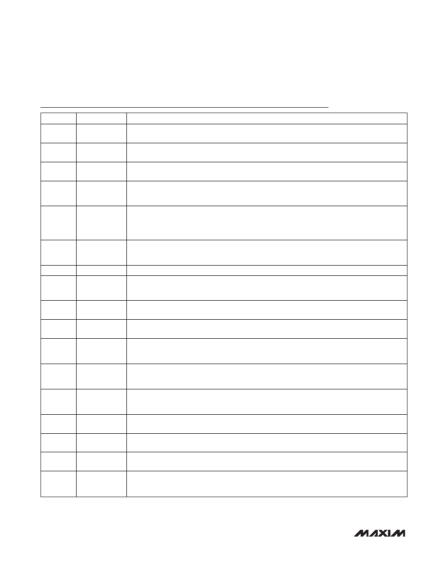
Pin Description
PIN
NAME
FUNCTION
1
P1.3/TCK
Port 1 Data 3/JTAG Serial Clock Input. P1.3 is a general-purpose digital I/O. TCK is the JTAG
serial test clock input. Refer to the MAXQ7667 User’s Guide Sections 5 and 11.
2
P1.4/MOSI
Port 1 Data 4/SPI Serial Data Output. P1.4 is a general-purpose digital I/O. MOSI is the master
output, slave input for the SPI interface. Refer to the MAXQ7667 User’s Guide Sections 5 and 9.
3
P1.5/MISO
Port 1 Data 5/SPI Serial Data Input. P1.5 is a general-purpose digital I/O. MISO is the master input,
slave output for the SPI interface. Refer to the MAXQ7667 User’s Guide Sections 5 and 9.
4
P1.6/SCLK
Port 1 Data 6/SPI Serial Clock Output. P1.6 is a general-purpose digital I/O. SCLK is the serial
clock for the SPI interface. SCLK is an input when operating as a slave and an output when
operating as a master. Refer to the MAXQ7667 User’s Guide Sections 5 and 9.
5
P1.7/SYNC/SS
Port 1 Data 7/Schedule Timer Sync Input/SPI Slave Select. P1.7 is a general-purpose digital I/O.
A rising edge on the SYNC input resets the schedule timer. In SPI slave mode, SS is the SPI
slave-select input. In SPI master mode, use SS or a GPIO to manually select an external slave.
Refer to the MAXQ7667 User’s Guide Sections 5, 7, and 9.
6, 19, 42
DVDD
Digital Supply Voltage. Connect DVDD directly to a +2.5V external source or to REG2P5 output for
single supply operation. Bypass DVDD to DGND with a 0.1F capacitor as close as possible to
the device. Connect all DVDD nodes together.
7, 18, 43
DGND
Digital Ground. Connect all DGND nodes together. Connect to AGND at a single point.
8, 17, 44
DVDDIO
Digital I/O Supply Voltage. DVDDIO powers all digital I/Os except for XIN and XOUT. Bypass
DVDDIO to DGND with a 0.1F capacitor as close as possible to the device. Connect all DVDDIO
nodes together.
9
P0.0/URX
Port 0 Data 0/UART Receive Data Input. P0.0 is a general-purpose digital I/O. URX is a UART or
LIN data receive input. Refer to the MAXQ7667 User’s Guide Sections 5 and 8.
10
P0.1/UTX
Port 0 Data 1/UART Transmit Data Output. P0.1 is a general-purpose digital I/O. UTX is a UART or
LIN data transmit output. Refer to the MAXQ7667 User’s Guide Sections 5 and 8.
11
P0.2/
TXEN
Port 0 Data 2/UART Transmit Output. P0.2 is a general-purpose digital I/O.
TXEN asserts low when
the UART is transmitting. Use
TXEN to enable an external LIN/UART transceiver. Refer to the
MAXQ7667 User’s Guide Sections 5 and 8.
12
P0.3/T0/
ADCCTL
Port 0 Data 3/Timer 0 I/O/ADC Control Input. P0.3 is a general-purpose digital I/O. T0 is the
primary Type 2 timer/counter 0 output or input. ADCCTL is a sampling/conversion trigger input for
the SAR ADC. Refer to the MAXQ7667 User’s Guide Sections 5, 6, and 14.
13
P0.4/T0B
Port 0 Data 4/Timer 0B I/O/Comparator Output. P0.4 is a general-purpose digital I/O. T0B is the
secondary Type 2 timer/counter 0 output or input. Refer to the MAXQ7667 User’s Guide Sections
5 and 6.
14
P0.5/T1
Port 0 Data 5/Timer 1 I/O. P0.5 is a general-purpose digital I/O. T1 is the primary Type 2
timer/counter 1 output or input. Refer to the MAXQ7667 User’s Guide Sections 5 and 6.
15
P0.6/T2
Port 0 Data 6/Timer 2 I/O. P0.6 is a general-purpose digital I/O. T2 is the primary Type 2
timer/counter 2 output or input. Refer to the MAXQ7667 User’s Guide Sections 5 and 6.
16
P0.7/T2B
Port 0 Data 7/Timer 2B I/O. P0.7 is a general-purpose digital I/O. T2B is the secondary Type 2
timer/counter 2 output or input. Refer to the MAXQ7667 User’s Guide Sections 5 and 6.
20
XIN
Crystal Oscillator Input. Connect an external crystal or resonator between XIN and XOUT. When
using an external clock source drive XIN with 2.5V level clock while leaving XOUT unconnected.
Connect XIN to DGND when an external clock source is not used.
相关PDF资料 |
PDF描述 |
|---|---|
| DS80C390-QCR+ | IC MPU CAN DUAL HS 68-PLCC |
| DS80C320-ENL+ | IC MCU HI SPEED 33MHZ IND 44TQFP |
| 221789-3 | CONN JACK VERT SMA PCB GOLD |
| 1408336-7 | CONN PLUG QMA R/A CRIMP RG-58 |
| DS5000FP-16+ | IC MODULE MICRO 16MHZ 80-QFP |
相关代理商/技术参数 |
参数描述 |
|---|---|
| MAXQ7667EVKIT | 功能描述:开发板和工具包 - 其他处理器 RoHS:否 制造商:Freescale Semiconductor 产品:Development Systems 工具用于评估:P3041 核心:e500mc 接口类型:I2C, SPI, USB 工作电源电压: |
| MAXQ7667EVKIT+ | 功能描述:开发板和工具包 - 其他处理器 MAXQ7667 Eval Kit RoHS:否 制造商:Freescale Semiconductor 产品:Development Systems 工具用于评估:P3041 核心:e500mc 接口类型:I2C, SPI, USB 工作电源电压: |
| MAXQ7667EVKIT-1# | 功能描述:开发板和工具包 - 其他处理器 MAXQ7667EVKIT-1# RoHS:否 制造商:Maxim Integrated 产品: 工具用于评估: 核心: 接口类型: 工作电源电压: |
| MAXQ7668AACM/V+ | 功能描述:16位微控制器 - MCU Integrated Circuits (ICs) Embedded - Microcontrollers - ADC 12BIT 8CH SER 2.7V LQFP RoHS:否 制造商:Texas Instruments 核心:RISC 处理器系列:MSP430FR572x 数据总线宽度:16 bit 最大时钟频率:24 MHz 程序存储器大小:8 KB 数据 RAM 大小:1 KB 片上 ADC:Yes 工作电源电压:2 V to 3.6 V 工作温度范围:- 40 C to + 85 C 封装 / 箱体:VQFN-40 安装风格:SMD/SMT |
| MAXQ7668AACM/V+T | 功能描述:16位微控制器 - MCU Integrated Circuits (ICs) Embedded - Microcontrollers - ADC 12BIT 8CH SER 2.7V LQFP RoHS:否 制造商:Texas Instruments 核心:RISC 处理器系列:MSP430FR572x 数据总线宽度:16 bit 最大时钟频率:24 MHz 程序存储器大小:8 KB 数据 RAM 大小:1 KB 片上 ADC:Yes 工作电源电压:2 V to 3.6 V 工作温度范围:- 40 C to + 85 C 封装 / 箱体:VQFN-40 安装风格:SMD/SMT |
发布紧急采购,3分钟左右您将得到回复。