- 您现在的位置:买卖IC网 > PDF目录10922 > MAXQ7670AATL/V+T (Maxim Integrated Products)IC MCU W/12BIT ADC 40TQFN-EP PDF资料下载
参数资料
| 型号: | MAXQ7670AATL/V+T |
| 厂商: | Maxim Integrated Products |
| 文件页数: | 6/38页 |
| 文件大小: | 0K |
| 描述: | IC MCU W/12BIT ADC 40TQFN-EP |
| 产品培训模块: | Lead (SnPb) Finish for COTS Obsolescence Mitigation Program |
| 标准包装: | 2,500 |
| 系列: | MAXQ® |
| 核心处理器: | RISC |
| 芯体尺寸: | 16-位 |
| 速度: | 16MHz |
| 连通性: | CAN,SPI |
| 外围设备: | 欠压检测/复位,POR,PWM,WDT |
| 输入/输出数: | 7 |
| 程序存储器容量: | 64KB(32K x 16) |
| 程序存储器类型: | 闪存 |
| RAM 容量: | 1K x 16 |
| 电压 - 电源 (Vcc/Vdd): | 2.25 V ~ 3.6 V |
| 数据转换器: | A/D 8x12b |
| 振荡器型: | 内部 |
| 工作温度: | -40°C ~ 125°C |
| 封装/外壳: | 40-WFQFN 裸露焊盘 |
| 包装: | 带卷 (TR) |
第1页第2页第3页第4页第5页当前第6页第7页第8页第9页第10页第11页第12页第13页第14页第15页第16页第17页第18页第19页第20页第21页第22页第23页第24页第25页第26页第27页第28页第29页第30页第31页第32页第33页第34页第35页第36页第37页第38页
MAXQ7670A
Microcontroller with 12-Bit ADC,
PGA, 64KB Flash, and CAN Interface
14
______________________________________________________________________________________
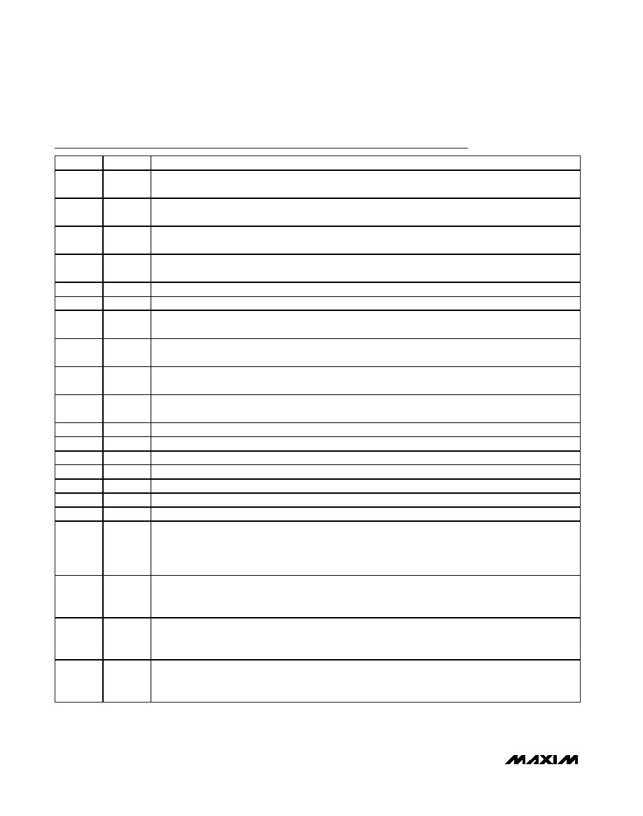
Pin Description
PIN
NAME
FUNCTION
1
AIN7
Analog Input Channel 7. AIN7 is multiplexed to the PGA or ADC as single-ended analog input 7 or as a
differential input with AIN6. As a differential input, the polarity of AIN7 is negative.
2
AIN6
Analog Input Channel 6. AIN6 is multiplexed to the PGA or ADC as a single-ended analog input 6 or as a
differential input with AIN7. As a differential input, the polarity of AIN6 is positive.
3
AIN5
Analog Input Channel 5. AIN5 is multiplexed to the PGA or ADC as single-ended analog input 5 or as a
differential input with AIN4. As a differential input, the polarity of AIN5 is negative.
4
AIN4
Analog Input Channel 4. AIN4 is multiplexed to the PGA or ADC as single-ended analog input 4 or as a
differential input with AIN5. As a differential input, the polarity of AIN4 is positive.
5
REFADC
ADC External Reference Input. Connect an external reference between 1V and VAVDD.
6
AGND
Analog Ground
7
AIN3
Analog Input Channel 3. AIN3 is multiplexed to the PGA or ADC as single-ended analog input 3 or as a
differential input with AIN2. As a differential input, the polarity of AIN3 is negative.
8
AIN2
Analog Input Channel 2. AIN2 is multiplexed to the PGA or ADC as single-ended analog input 2 or as a
differential input with AIN3. As a differential input, the polarity of AIN2 is positive.
9
AIN1
Analog Input Channel 1. AIN1 is multiplexed to the PGA or ADC as single-ended analog input 1 or as a
differential input with AIN0. As a differential input, the polarity of AIN1 is negative.
10
AIN0
Analog Input Channel 0. AIN0 is multiplexed to the PGA or ADC as single-ended analog input 0 or as a
differential input with AIN1. As a differential input, the polarity of AIN0 is positive.
11
I.C.
Internally Connected. Connect to GNDIO for proper operation.
12
P0.0
Port 0 Bit 0. P0.0 is a general-purpose digital I/O with interrupt/wake-up capability.
13
P0.1
Port 0 Bit 1. P0.1 is a general-purpose digital I/O with interrupt/wake-up capability.
14
P0.2
Port 0 Bit 2. P0.2 is a general-purpose digital I/O with interrupt/wake-up capability.
15, 22, 38
GNDIO
Digital I/O Ground and Regulator Ground
16
CANRXD
CAN Bus Receiver Input. CAN receiver input.
17
CANTXD
CAN Bus Transmitter Output. CAN transmitter output.
18
SS
Active-Low, SPI Port Slave Select Input. In SPI slave mode, this is the slave select input. In SPI master
mode, this is an input and connection is optional (connect if mode fault enable is required, refer to the
MAXQ7670 User’s Guide for a description of the SPICN register). In master mode, use an available GPIO
as a slave selector and pull SS high to DVDDIO through a pullup resistor.
19
P0.6/T0
Port 0 Bit 6/Timer 0 I/O. P0.6 is a general-purpose digital I/O with interrupt/wake-up input capability. T0 is a
primary timer/PWM input or output. The alternative function, T0, is selected using the T2CNA0 register.
When this function is selected, it overrides the GPIO functionality.
20
P0.7/T0B
Port 0 Bit 7/Timer 0 Output. P0.7 is a general-purpose digital I/O with interrupt/wake-up input capability.
T0B is a secondary timer/PWM output. The alternative function, T0B, is selected using the T2CNB0 register.
When this function is selected, it overrides the GPIO functionality.
21, 39
DVDDIO
Digital I/O Supply Voltage and Regulator Supply Input. DVDDIO supplies all digital I/O except for XIN and
XOUT, and supplies power to the two internal linear regulators, AVDD and DVDD. Bypass DVDDIO to
GNDIO with a 0.1F capacitor as close as possible to the device.
相关PDF资料 |
PDF描述 |
|---|---|
| VE-26M-CV-S | CONVERTER MOD DC/DC 10V 150W |
| MAXQ7670ATL+T | IC MCU W/10BIT ADC 40TQFN-EP |
| 73S1210F-68IM/F | IC SMART CARD READER 68-QFN |
| ISD17180EYI | IC VOICE REC/PLAY 180SEC 28-TSOP |
| ISD17150SY | IC VOICE REC/PLAY 150SEC 28-SOIC |
相关代理商/技术参数 |
参数描述 |
|---|---|
| MAXQ7670ATL/V+ | 功能描述:16位微控制器 - MCU MCU w/12-Bit ADC PGA 64KB Flash & CAN Int RoHS:否 制造商:Texas Instruments 核心:RISC 处理器系列:MSP430FR572x 数据总线宽度:16 bit 最大时钟频率:24 MHz 程序存储器大小:8 KB 数据 RAM 大小:1 KB 片上 ADC:Yes 工作电源电压:2 V to 3.6 V 工作温度范围:- 40 C to + 85 C 封装 / 箱体:VQFN-40 安装风格:SMD/SMT |
| MAXQ7670ATL/V+T | 功能描述:16位微控制器 - MCU MCU w/12-Bit ADC PGA 64KB Flash & CAN Int RoHS:否 制造商:Texas Instruments 核心:RISC 处理器系列:MSP430FR572x 数据总线宽度:16 bit 最大时钟频率:24 MHz 程序存储器大小:8 KB 数据 RAM 大小:1 KB 片上 ADC:Yes 工作电源电压:2 V to 3.6 V 工作温度范围:- 40 C to + 85 C 封装 / 箱体:VQFN-40 安装风格:SMD/SMT |
| MAXQ7670ATL+ | 功能描述:16位微控制器 - MCU MCU w/12-Bit ADC PGA 64KB Flash & CAN Int RoHS:否 制造商:Texas Instruments 核心:RISC 处理器系列:MSP430FR572x 数据总线宽度:16 bit 最大时钟频率:24 MHz 程序存储器大小:8 KB 数据 RAM 大小:1 KB 片上 ADC:Yes 工作电源电压:2 V to 3.6 V 工作温度范围:- 40 C to + 85 C 封装 / 箱体:VQFN-40 安装风格:SMD/SMT |
| MAXQ7670ATL+T | 功能描述:16位微控制器 - MCU MCU w/12-Bit ADC PGA 64KB Flash & CAN Int RoHS:否 制造商:Texas Instruments 核心:RISC 处理器系列:MSP430FR572x 数据总线宽度:16 bit 最大时钟频率:24 MHz 程序存储器大小:8 KB 数据 RAM 大小:1 KB 片上 ADC:Yes 工作电源电压:2 V to 3.6 V 工作温度范围:- 40 C to + 85 C 封装 / 箱体:VQFN-40 安装风格:SMD/SMT |
| MAXQ7670EVKIT+ | 功能描述:开发板和工具包 - 其他处理器 MAXQ7670 Eval Kit RoHS:否 制造商:Freescale Semiconductor 产品:Development Systems 工具用于评估:P3041 核心:e500mc 接口类型:I2C, SPI, USB 工作电源电压: |
发布紧急采购,3分钟左右您将得到回复。