- 您现在的位置:买卖IC网 > PDF目录17100 > MAXQ7670EVKIT+ (Maxim Integrated Products)KIT EVAL FOR MAXQ7670 PDF资料下载
参数资料
| 型号: | MAXQ7670EVKIT+ |
| 厂商: | Maxim Integrated Products |
| 文件页数: | 7/38页 |
| 文件大小: | 0K |
| 描述: | KIT EVAL FOR MAXQ7670 |
| 产品培训模块: | Lead (SnPb) Finish for COTS Obsolescence Mitigation Program |
| 标准包装: | 1 |
| 系列: | MAXQ® |
| 类型: | MCU |
| 适用于相关产品: | MAXQ7670 |
| 所含物品: | 板 |
第1页第2页第3页第4页第5页第6页当前第7页第8页第9页第10页第11页第12页第13页第14页第15页第16页第17页第18页第19页第20页第21页第22页第23页第24页第25页第26页第27页第28页第29页第30页第31页第32页第33页第34页第35页第36页第37页第38页
MAXQ7670
Microcontroller with 10-Bit ADC,
PGA, 64KB Flash, and CAN Interface
______________________________________________________________________________________
15
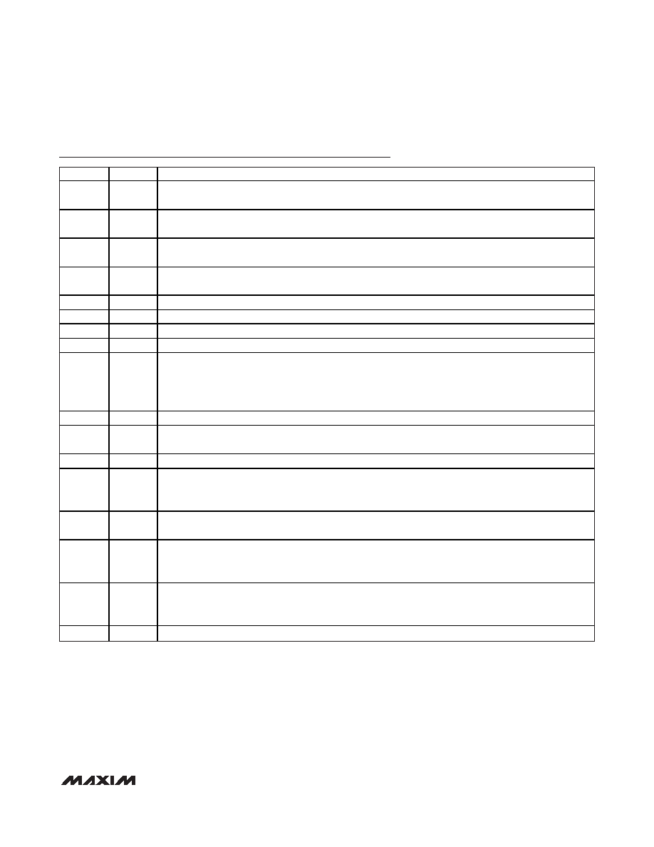
Pin Description (continued)
PIN
NAME
FUNCTION
23
SCLK
SPI Serial Clock. SCLK is the SPI interface serial clock I/O. In SPI master mode, SCLK is an output. While in
SPI slave mode, SCLK is an input.
24
MOSI
SPI Serial Data I/O. MOSI is the SPI interface serial data output in master mode or serial data input in slave
mode.
25
MISO
SPI Serial Data I/O. MISO is the SPI interface serial data input in master mode or serial data output in slave
mode.
26
REGEN2
Active-Low +2.5V Linear Regulator Enable Input. Connect
REGEN2 to GNDIO to enable the +2.5V linear
regulator. Connect to DVDDIO to disable the +2.5V linear regulator.
27
TDO
JTAG Serial Test Data Output. TDO is the JTAG serial test, data output.
28
TMS
JTAG Test Mode Select. TMS is the JTAG test mode, select input.
29
TDI
JTAG Serial Test Data Input. TDI is the JTAG serial test, data input.
30
TCK
JTAG Serial Test Clock Input. TCK is the JTAG serial test, clock input.
31
P0.4/
ADCCNV
Port 0 Bit 4/ADC Start Conversion Control. P0.4 is a general-purpose digital I/O with interrupt/wake-up
capability. ADCCNV is a firmware-configurable, rising or falling edge, start/convert signal used to trigger
ADC conversions. The alternative function, ADCCNV, is selected using the register bits ACNT[2:0]. When
using ADCCNV as a trigger for ADC conversion, set P0.4/ADCCNV as an input using the PD0 register. This
action prevents any unintentional interference in the SARADC operation.
32
P0.5
Port 0 Bit 5. P0.5 is a general-purpose digital I/O with interrupt/wake-up capability.
33
RESET
Reset Input/Output. Active-low input/output with internal 55k
pullup to DVDDIO. Drive low to reset the
MAXQ7670. The MAXQ20 C core holds
RESET low during POR and during DVDD brownout conditions.
34
DGND
Digital Ground
35
XOUT
High-Frequency Crystal Output. Connect an external crystal to XIN and XOUT for normal operation, or leave
unconnected if XIN is driven with an external clock source. Leave unconnected if an external clock source
is not used.
36
XIN
High-Frequency Crystal Input. Connect an external crystal or resonator to XIN and XOUT for normal operation,
or drive XIN with an external clock source. Leave unconnected if an external clock source is not used.
37
DVDD
Digital Supply Voltage. DVDD supplies internal digital core and flash memory. DVDD is directly connected to
the output of the internal +2.5V linear regulator. Disable the internal regulator (through
REGEN2) to connect an
external supply. Bypass DVDD to DGND with a 0.1F capacitor as close as possible to the device.
40
AVDD
Analog Supply Voltage. AVDD supplies PGA and ADC. AVDD is directly connected to the output of the
internal +3.3V linear regulator. Disable the internal regulator (via software) to connect an external supply.
Bypass AVDD to AGND with a 0.1F capacitor as close as possible to the device.
—
EP
Exposed Pad. Connect EP to the ground plane.
相关PDF资料 |
PDF描述 |
|---|---|
| EBC28DRYS | CONN EDGECARD 56POS DIP .100 SLD |
| EBC26DRYI | CONN EDGECARD 52POS DIP .100 SLD |
| SCRH6D28-100 | INDUCTOR SMD 10UH 1.70A 10KHZ |
| EEC43DRTS | CONN EDGECARD 86POS DIP .100 SLD |
| EBC31DRTS | CONN EDGECARD 62POS DIP .100 SLD |
相关代理商/技术参数 |
参数描述 |
|---|---|
| MAXQ7670EVKIT+ | 功能描述:开发板和工具包 - 其他处理器 MAXQ7670 Eval Kit RoHS:否 制造商:Freescale Semiconductor 产品:Development Systems 工具用于评估:P3041 核心:e500mc 接口类型:I2C, SPI, USB 工作电源电压: |
| MAXQ8913 | 制造商:MAXIM 制造商全称:Maxim Integrated Products 功能描述:16-Bit, Mixed-Signal Microcontroller with Op Amps, ADC, and DACs for All-in-One Servo Loop Control |
| MAXQ8913EWG+T | 制造商:MAXIM 制造商全称:Maxim Integrated Products 功能描述:16-Bit, Mixed-Signal Microcontroller with Op Amps, ADC, and DACs for All-in-One Servo Loop Control |
| MAXQ8913EWG-T&R+ | 制造商:Maxim Integrated Products 功能描述:MAXQ8913 IMAGE STABILIZER WLF T&R - Gel-pak, waffle pack, wafer, diced wafer on film |
| MAXQ8913X-0000+ | 功能描述:16位微控制器 - MCU 16-Bit Mxd Sgnl MCU w/Op Amp ADC & DAC RoHS:否 制造商:Texas Instruments 核心:RISC 处理器系列:MSP430FR572x 数据总线宽度:16 bit 最大时钟频率:24 MHz 程序存储器大小:8 KB 数据 RAM 大小:1 KB 片上 ADC:Yes 工作电源电压:2 V to 3.6 V 工作温度范围:- 40 C to + 85 C 封装 / 箱体:VQFN-40 安装风格:SMD/SMT |
发布紧急采购,3分钟左右您将得到回复。