- 您现在的位置:买卖IC网 > PDF目录229297 > MB84VD22184EA-90PBS SPECIALTY MEMORY CIRCUIT, PBGA71 PDF资料下载
参数资料
| 型号: | MB84VD22184EA-90PBS |
| 元件分类: | 存储器 |
| 英文描述: | SPECIALTY MEMORY CIRCUIT, PBGA71 |
| 封装: | PLASTIC, BGA-71 |
| 文件页数: | 27/64页 |
| 文件大小: | 1177K |
| 代理商: | MB84VD22184EA-90PBS |
第1页第2页第3页第4页第5页第6页第7页第8页第9页第10页第11页第12页第13页第14页第15页第16页第17页第18页第19页第20页第21页第22页第23页第24页第25页第26页当前第27页第28页第29页第30页第31页第32页第33页第34页第35页第36页第37页第38页第39页第40页第41页第42页第43页第44页第45页第46页第47页第48页第49页第50页第51页第52页第53页第54页第55页第56页第57页第58页第59页第60页第61页第62页第63页第64页
MB84VD2218XEA/H/2219XEA/H-70/85/90
33
(Continued)
*1: Both Read/Reset commands are functionally equivalent, resetting the device to the read mode.
*2: This command is valid during Fast Mode.
*3: This command is valid while RESET
= VID.
*4: Valid Address is A6 to A0.
*5: This command is valid during Hi-ROM mode.
*6: The data “00h” is also acceptable.
Note : The command combinations not described in Command Definitions are illegal.
Address bits A20 to A11
= X = “H” or “L” for all address commands except for Program Address (PA) ,
Sector Address (SA) , and Bank Address (BA) .
Bus operations are defined in s DEVICE BUS OPERATION “User Bus Operations” Table.
RA
= Address of the memory location to be read.
PA
= Address of the memory location to be programmed.
Addresses are latched on the falling edge of the write pulse.
SA
= Address of the sector to be erased. The combination of A20, A19, A18, A17, A16, A15, A14, A13, and A12 will
uniquely select any sector.
BA
= Bank address (A20 to A15)
SPA
= Sector group address to be protected. Set sector group address (SPA) and (A6, A1, A0) = (0, 1, 0) .
HRA
= Address of the Hidden-ROM area.
MB84VD2218XEA/H (Top Boot Type)
Word mode : 1F8000h to 1FFFFFh
Byte mode : 3F0000h to 3FFFFFh
MB84VD2219XEA/H (Bottom Boot Type) Word mode : 000000h to 007FFFh
Byte mode : 000000h to 00FFFFh
HRBA
= Bank address of the Hidden-ROM area
MB84VD2218XEA/H (Top Boot Type)
: A20
= A19 = A18 = A17 = A16 = A15 = 1
MB84VD2219XEA/H (Bottom Boot Type) : A20
= A19 = A18 = A17 = A16 = A15 = 0
RD
= Data read from location RA during read operation.
PD
= Data to be programmed at location PA.
SD
= Sector protection verify data. Output 01h at protected sector addresses and output 00h
at unprotectedsector addresses.
The system should generate the following address patterns :
Word mode : 555h or 2AAh to addresses A10 to A0
Byte mode : AAAh or 555h to addresses A10 to A0 and A-1
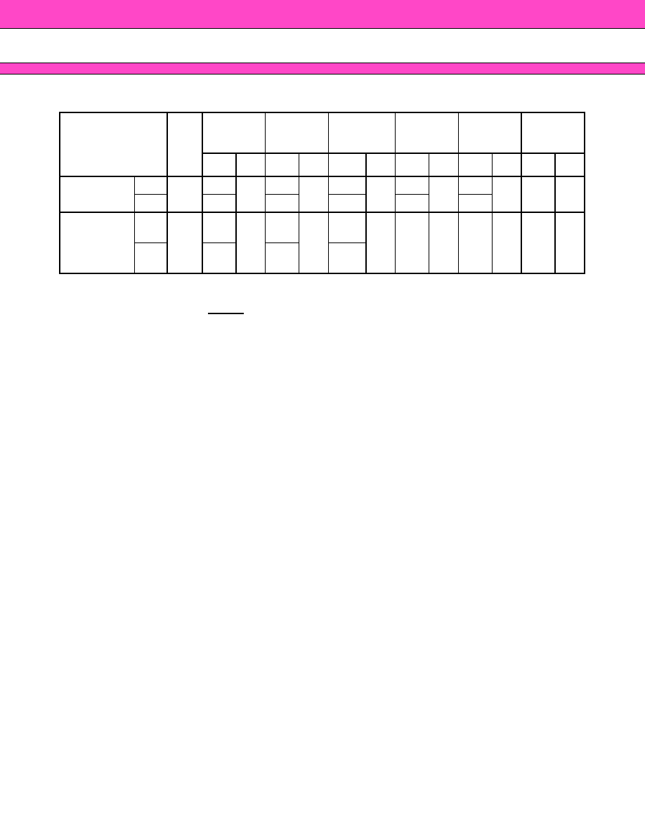
Command
Sequence
Bus
Write
Cy-
cles
Req’d
First Bus
Write Cycle
Second
Bus
Write Cycle
Third Bus
Write Cycle
Fourth Bus
Read/Write
Cycle
Fifth Bus
Write Cycle
Sixth Bus
Write Cycle
Addr. Data Addr. Data Addr. Data Addr. Data Addr. Data Addr. Data
Hi-ROM Erase
*5
Word
6
555h
AAh
2AAh
55h
555h
80h
555h
AAh
2AAh
55h
HRA
30h
Byte
AAAh
555h
AAAh
555h
Hi-ROM Exit *5
Word
4
555h
AAh
2AAh
55h
(HRBA)
555h
90h XXXh 00h
Byte
AAAh
555h
(HRBA)
AAAh
相关PDF资料 |
PDF描述 |
|---|---|
| M93C66-WMB3TP | 256 X 16 MICROWIRE BUS SERIAL EEPROM, DSO8 |
| MT48LC4M16A2P-75:G | 4M X 16 SYNCHRONOUS DRAM, 5.4 ns, PDSO54 |
| M93C06-MB6G | 16 X 16 MICROWIRE BUS SERIAL EEPROM, DSO8 |
| MT48LC4M16A2F4-6IT:G | 4M X 16 SYNCHRONOUS DRAM, 5.5 ns, PBGA54 |
| MT46V32M8FG-6TIT:G | 32M X 8 DDR DRAM, 0.7 ns, PBGA60 |
相关代理商/技术参数 |
参数描述 |
|---|---|
| MB84VD22184EC | 制造商:FUJITSU 制造商全称:Fujitsu Component Limited. 功能描述:32M (x 8/x16) FLASH MEMORY & 4M (x 8/x16) STATIC RAM |
| MB84VD22184EC-90 | 制造商:FUJITSU 制造商全称:Fujitsu Component Limited. 功能描述:32M (x 8/x16) FLASH MEMORY & 4M (x 8/x16) STATIC RAM |
| MB84VD22184EC-90-PBS | 制造商:FUJITSU 制造商全称:Fujitsu Component Limited. 功能描述:32M (x 8/x16) FLASH MEMORY & 4M (x 8/x16) STATIC RAM |
| MB84VD22184EE | 制造商:FUJITSU 制造商全称:Fujitsu Component Limited. 功能描述:32M (x 8/x16) FLASH MEMORY & 4M (x 8/x16) STATIC RAM |
| MB84VD22184EE-90 | 制造商:FUJITSU 制造商全称:Fujitsu Component Limited. 功能描述:32M (x 8/x16) FLASH MEMORY & 4M (x 8/x16) STATIC RAM |
发布紧急采购,3分钟左右您将得到回复。