- 您现在的位置:买卖IC网 > PDF目录45188 > MB90671PFV 16-BIT, MROM, 16 MHz, MICROCONTROLLER, PQFP80 PDF资料下载
参数资料
| 型号: | MB90671PFV |
| 元件分类: | 微控制器/微处理器 |
| 英文描述: | 16-BIT, MROM, 16 MHz, MICROCONTROLLER, PQFP80 |
| 封装: | PLASTIC, LQFP-80 |
| 文件页数: | 40/106页 |
| 文件大小: | 1648K |
| 代理商: | MB90671PFV |
第1页第2页第3页第4页第5页第6页第7页第8页第9页第10页第11页第12页第13页第14页第15页第16页第17页第18页第19页第20页第21页第22页第23页第24页第25页第26页第27页第28页第29页第30页第31页第32页第33页第34页第35页第36页第37页第38页第39页当前第40页第41页第42页第43页第44页第45页第46页第47页第48页第49页第50页第51页第52页第53页第54页第55页第56页第57页第58页第59页第60页第61页第62页第63页第64页第65页第66页第67页第68页第69页第70页第71页第72页第73页第74页第75页第76页第77页第78页第79页第80页第81页第82页第83页第84页第85页第86页第87页第88页第89页第90页第91页第92页第93页第94页第95页第96页第97页第98页第99页第100页第101页第102页第103页第104页第105页第106页
MB90670/675 Series
39
s PERIPHERALS
1.
I/O Port
(1) Input/output Port
Port 0 to 4, 6, 8, A, and B are general-purpose I/O ports having a combined function as an external bus pin and
a resource input. The input output ports function as general-purpose I/O port only in the single-chip mode. In
the external bus mode, the ports are configured as external bus pins, and part of pins for port 3 can be configured
as general-purpose I/O port by setting the bus control signal select register (ECSR). Each pin corresponding
to upper 4-bit of the port 2 can be switched between a resource and a port bitwise.
Only MB90675 series has port A and port B.
Operation as output port
The pin is configured as an output port by setting the corresponding bit of the DDR register to “1”.
Writing data to PDR register when the port is configured as output, the data is retained in the output latch in
the PDR and directly output to the pin.
The value of the pin (the same value retained in the output latch of PDR) can be read out by reading the PDR
register.
Note: When a read-modify-write instruction (e.g. bit set instruction) is performed to the port data register, the
destination bit of the operation is set to the specified value, not affecting the bits configured by the
DDR register for output, however, values of bits configured by the DDR register as inputs are changed
because input values to the pins are written into the output latch. To avoid this situation, configure the
pins by the DDR register as output after writing output data to the PDR register when configuring the
bit used as input as outputs.
Operation as input port
The pin is configured as an input by setting the corresponding bit of the DDR register to “0”.
When the pin is configured as an input, the output buffer is turned-off and the pin is put into a high-impedance
status.
When a data is written into the PDR register, the data is retained in the output latch of the PDR, but pin outputs
are unaffected.
Reading the PDR register reads out the pin level (“0” or “1”)
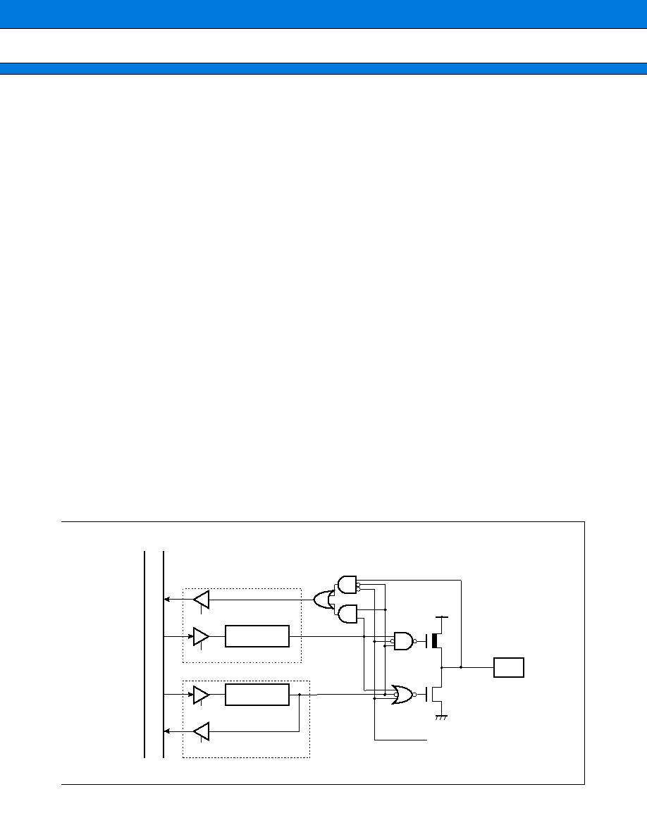
Block diagram
PDR (port data register)
DDR (port direction register)
PDR read
PDR write
DDR write
DDR read
Direction latch
Output latch
Internal
data
bus
Standby control: Stop, timebase timer mode and SPL=1, or hardware standby mode
Standby control (SPL=1)
P-ch
N-ch
Pin
相关PDF资料 |
PDF描述 |
|---|---|
| MB90671PF | 16-BIT, MROM, 16 MHz, MICROCONTROLLER, PQFP80 |
| MB90P678PF | 16-BIT, OTPROM, 16 MHz, MICROCONTROLLER, PQFP100 |
| MB90T673PFV | 16-BIT, 16 MHz, MICROCONTROLLER, PQFP80 |
| MB90P673PFV | 16-BIT, OTPROM, 16 MHz, MICROCONTROLLER, PQFP80 |
| MB90P673PF | 16-BIT, OTPROM, 16 MHz, MICROCONTROLLER, PQFP80 |
相关代理商/技术参数 |
参数描述 |
|---|---|
| MB90672 | 制造商:FUJITSU 制造商全称:Fujitsu Component Limited. 功能描述:16-Bit Proprietary Microcontroller |
| MB90672PF | 制造商:FUJITSU 制造商全称:Fujitsu Component Limited. 功能描述:16-Bit Proprietary Microcontroller |
| MB90672PFV | 制造商:FUJITSU 制造商全称:Fujitsu Component Limited. 功能描述:16-Bit Proprietary Microcontroller |
| MB90673 | 制造商:FUJITSU 制造商全称:Fujitsu Component Limited. 功能描述:16-Bit Proprietary Microcontroller |
| MB90673PF | 制造商:FUJITSU 制造商全称:Fujitsu Component Limited. 功能描述:16-Bit Proprietary Microcontroller |
发布紧急采购,3分钟左右您将得到回复。