- 您现在的位置:买卖IC网 > PDF目录69020 > MB90F334APFF 16-BIT, FLASH, 24 MHz, MICROCONTROLLER, PQFP120 PDF资料下载
参数资料
| 型号: | MB90F334APFF |
| 元件分类: | 微控制器/微处理器 |
| 英文描述: | 16-BIT, FLASH, 24 MHz, MICROCONTROLLER, PQFP120 |
| 封装: | 14 X 14 MM, 1.70 MM HEIGHT, 0.40 MM PITCH, PLASTIC, LFQFP-120 |
| 文件页数: | 111/120页 |
| 文件大小: | 1210K |
| 代理商: | MB90F334APFF |
第1页第2页第3页第4页第5页第6页第7页第8页第9页第10页第11页第12页第13页第14页第15页第16页第17页第18页第19页第20页第21页第22页第23页第24页第25页第26页第27页第28页第29页第30页第31页第32页第33页第34页第35页第36页第37页第38页第39页第40页第41页第42页第43页第44页第45页第46页第47页第48页第49页第50页第51页第52页第53页第54页第55页第56页第57页第58页第59页第60页第61页第62页第63页第64页第65页第66页第67页第68页第69页第70页第71页第72页第73页第74页第75页第76页第77页第78页第79页第80页第81页第82页第83页第84页第85页第86页第87页第88页第89页第90页第91页第92页第93页第94页第95页第96页第97页第98页第99页第100页第101页第102页第103页第104页第105页第106页第107页第108页第109页第110页当前第111页第112页第113页第114页第115页第116页第117页第118页第119页第120页
MB90330A Series
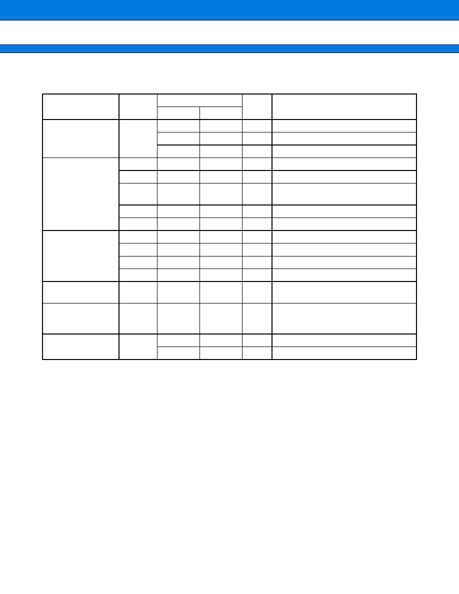
90
2.
Recommended Operating Conditions
(VSS
= AVSS = 0.0 V)
* : Applicable to pins : P60 to P67, P96, PA0 to PA7, PB0 to PB4, UTEST
WARNING: The recommended operating conditions are required in order to ensure the normal operation of the
semiconductor device. All of the device’s electrical characteristics are warranted when the device is
operated within these ranges.
Always use semiconductor devices within their recommended operating condition ranges. Operation
outside these ranges may adversely affect reliability and could result in device failure.
No warranty is made with respect to uses, operating conditions, or combinations not represented on
the data sheet. Users considering application outside the listed conditions are advised to contact their
FUJITSU representatives beforehand.
Parameter
Symbol
Value
Unit
Remarks
Min
Max
Power supply voltage
VCC
3.0
3.6
V
At normal operation (when using USB)
2.7
3.6
V
At normal operation (when not using USB)
1.8
3.6
V
Hold state of stop operation
Input “H” voltage
VIH
0.7 VCC
VCC
+ 0.3
V
CMOS input pin
VIHS1
0.8 VCC
VCC
+ 0.3
V
CMOS hysteresis input pin
VIHS2
0.8 VCC
VSS
+ 5.3
V
N-ch open-drain
(Withstand voltage of 5 V I/O)*
VIHM
VCC
0.3
VCC
+ 0.3
V
MD pin input
VIHUSB
2.0
VCC
+ 0.3
V
USB pin input
Input “L” voltage
VIL
VSS
0.3
0.3 VCC
V
CMOS input pin
VILS
VSS
0.3
0.2 VCC
V
CMOS hysteresis input pin
VILM
VSS
0.3
VSS
+ 0.3
V
MD pin input
VILUSB
VSS
0.8
V
USB pin input
Differential input
sensitivity
VDI
0.2
V
USB pin input
Differential common
mode input voltage
range
VCM
0.8
2.5
V
USB pin input
Operating
temperature
TA
40
+ 85
°C
When not using USB
0
+ 70
°C
When using USB
相关PDF资料 |
PDF描述 |
|---|---|
| MB90F334APMC | 16-BIT, FLASH, 24 MHz, MICROCONTROLLER, PQFP120 |
| MB90333APMC | 16-BIT, MROM, 24 MHz, MICROCONTROLLER, PQFP120 |
| MB90F334APMC1 | 16-BIT, FLASH, 24 MHz, MICROCONTROLLER, PQFP120 |
| MB90F395HAPMT | 16-BIT, FLASH, 24 MHz, MICROCONTROLLER, PQFP120 |
| MB90F428GBPFV | 16-BIT, FLASH, 16 MHz, MICROCONTROLLER, PQFP100 |
相关代理商/技术参数 |
参数描述 |
|---|---|
| MB90F334APMC1-GE1 | 制造商:FUJITSU 功能描述: |
| MB90F334APMC1-G-SPE1 | 制造商:FUJITSU 功能描述: |
| MB90F334APMC-G-JNE1 | 制造商:FUJITSU 功能描述: |
| MB90F334APMC-G-SNE1 | 制造商:FUJITSU 功能描述: |
| MB90F334APMC-G-SPE1 | 制造商:FUJITSU 功能描述: |
发布紧急采购,3分钟左右您将得到回复。