- 您现在的位置:买卖IC网 > PDF目录132984 > MB9AF311LPMC1 32-BIT, FLASH, 40 MHz, RISC MICROCONTROLLER, PQFP64 PDF资料下载
参数资料
| 型号: | MB9AF311LPMC1 |
| 元件分类: | 微控制器/微处理器 |
| 英文描述: | 32-BIT, FLASH, 40 MHz, RISC MICROCONTROLLER, PQFP64 |
| 封装: | 0.50 MM PITCH, PLASTIC, LQFP-64 |
| 文件页数: | 103/114页 |
| 文件大小: | 1357K |
| 代理商: | MB9AF311LPMC1 |
第1页第2页第3页第4页第5页第6页第7页第8页第9页第10页第11页第12页第13页第14页第15页第16页第17页第18页第19页第20页第21页第22页第23页第24页第25页第26页第27页第28页第29页第30页第31页第32页第33页第34页第35页第36页第37页第38页第39页第40页第41页第42页第43页第44页第45页第46页第47页第48页第49页第50页第51页第52页第53页第54页第55页第56页第57页第58页第59页第60页第61页第62页第63页第64页第65页第66页第67页第68页第69页第70页第71页第72页第73页第74页第75页第76页第77页第78页第79页第80页第81页第82页第83页第84页第85页第86页第87页第88页第89页第90页第91页第92页第93页第94页第95页第96页第97页第98页第99页第100页第101页第102页当前第103页第104页第105页第106页第107页第108页第109页第110页第111页第112页第113页第114页
89
ATmega48PA/88PA/168PA [DATASHEET]
9223F–AVR–04/14
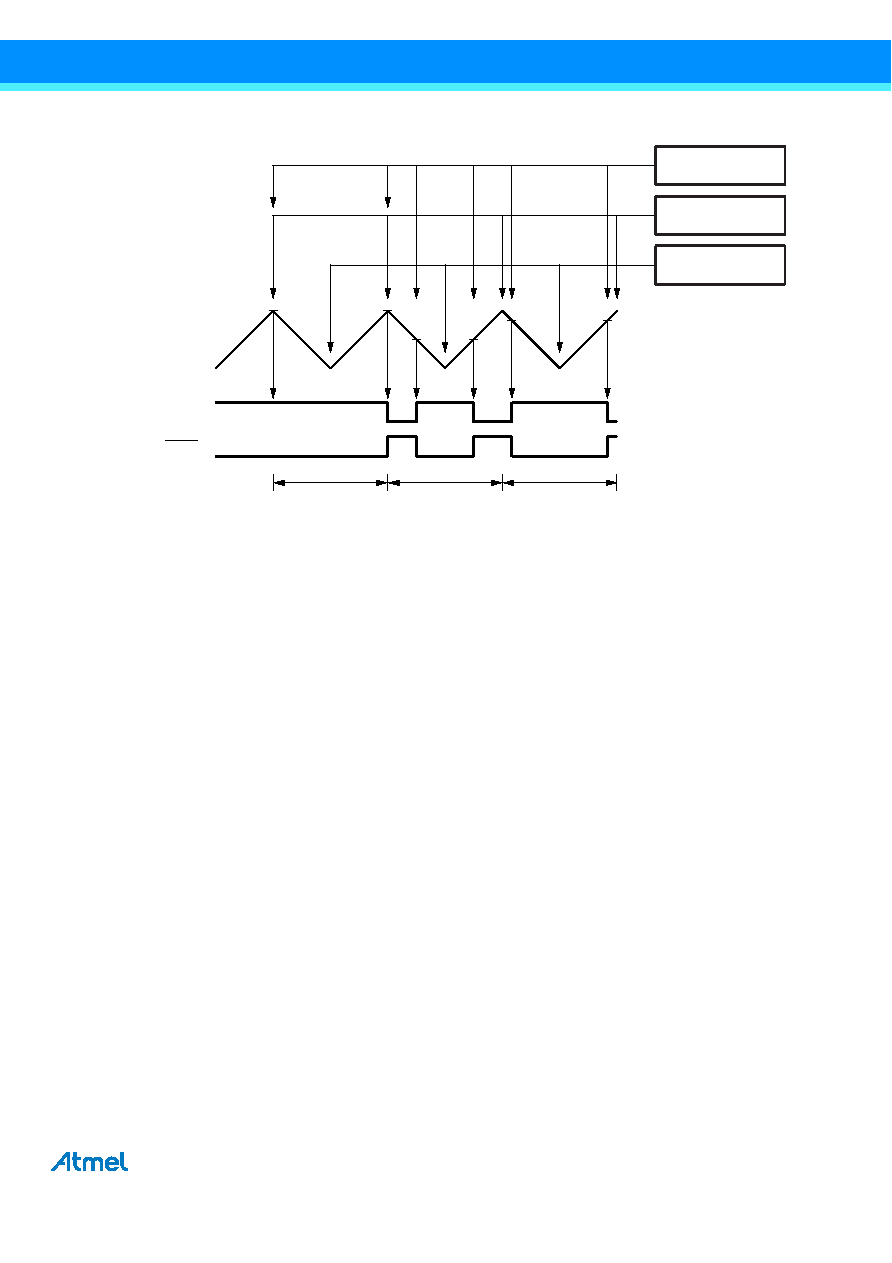
Figure 15-7. Phase Correct PWM Mode, Timing Diagram
The Timer/Counter overflow flag (TOV0) is set each time the counter reaches BOTTOM. The interrupt flag can be used to
generate an interrupt each time the counter reaches the BOTTOM value.
In phase correct PWM mode, the compare unit allows generation of PWM waveforms on the OC0x pins. Setting the
COM0x1:0 bits to two will produce a non-inverted PWM. An inverted PWM output can be generated by setting the
COM0x1:0 to three: Setting the COM0A0 bits to one allows the OC0A pin to toggle on compare matches if the WGM02 bit is
set. This option is not available for the OC0B pin (see Table 15-7 on page 93). The actual OC0x value will only be visible on
the port pin if the data direction for the port pin is set as output. The PWM waveform is generated by clearing (or setting) the
OC0x register at the compare match between OCR0x and TCNT0 when the counter increments, and setting (or clearing) the
OC0x register at compare match between OCR0x and TCNT0 when the counter decrements. The PWM frequency for the
output when using phase correct PWM can be calculated by the following equation:
The N variable represents the prescale factor (1, 8, 64, 256, or 1024).
The extreme values for the OCR0A register represent special cases when generating a PWM waveform output in the phase
correct PWM mode. If the OCR0A is set equal to BOTTOM, the output will be continuously low and if set equal to MAX the
output will be continuously high for non-inverted PWM mode. For inverted PWM the output will have the opposite logic
values.
At the very start of period 2 in Figure 15-7 OCnx has a transition from high to low even though there is no compare match.
The point of this transition is to guarantee symmetry around BOTTOM. There are two cases that give a transition without
compare match.
●
OCRnx changes its value from MAX, like in Figure 15-7. When the OCR0A value is MAX the OCn pin value is the
same as the result of a down-counting compare match. To ensure symmetry around BOTTOM the OCnx value at
MAX must correspond to the result of an up-counting compare match.
●
The timer starts counting from a value higher than the one in OCRnx, and for that reason misses the compare match
and hence the OCnx change that would have happened on the way up.
123
TCNTn
(COMnx1:0 = 2)
(COMnx1:0 = 3)
OCnx
Period
TOVn Interrupt
Flag Set
OCRnx Update
OCnx Interrupt
Flag Set
fOCnxPCPWM
fclk_I/O
N 510
×
-------------------
=
相关PDF资料 |
PDF描述 |
|---|---|
| MB9AF311MPMC | 32-BIT, FLASH, 40 MHz, RISC MICROCONTROLLER, PQFP80 |
| MSP430G2152IRSA16 | 16-BIT, FLASH, 16 MHz, RISC MICROCONTROLLER, PQCC16 |
| M37704E2EFP | 16-BIT, OTPROM, 16 MHz, MICROCONTROLLER, PQFP80 |
| MSM65544-JS | 8-BIT, MROM, 10 MHz, MICROCONTROLLER, PQCC68 |
| MSM65516SS | 8-BIT, MROM, 10 MHz, MICROCONTROLLER, PDIP64 |
相关代理商/技术参数 |
参数描述 |
|---|---|
| MB9AF312KPMC1-G-JNE2 | 功能描述:ARM? Cortex?-M3 FM3 MB9A310K Microcontroller IC 32-Bit 40MHz 160KB (160K x 8) FLASH 52-LQFP (10x10) 制造商:cypress semiconductor corp 系列:FM3 MB9A310K 包装:托盘 零件状态:有效 核心处理器:ARM? Cortex?-M3 核心尺寸:32-位 速度:40MHz 连接性:CSIO,I2C,LIN,UART/USART,USB 外设:DMA,LVD,POR,PWM,WDT I/O 数:36 程序存储容量:160KB(160K x 8) 程序存储器类型:闪存 EEPROM 容量:- RAM 容量:16K x 8 电压 - 电源(Vcc/Vdd):2.7 V ~ 5.5 V 数据转换器:A/D 8x12b 振荡器类型:内部 工作温度:-40°C ~ 105°C(TA) 封装/外壳:52-LQFP 供应商器件封装:52-LQFP(10x10) 标准包装:160 |
| MB9AF312KPMC-ES-E1 | 制造商:FUJITSU 功能描述: |
| MB9AF312KPMC-G-JNE1 | 制造商:FUJITSU 功能描述: |
| MB9AF312KPMC-G-JNE2 | 功能描述:ARM? Cortex?-M3 FM3 MB9A310K Microcontroller IC 32-Bit 40MHz 160KB (160K x 8) FLASH 48-LQFP (7x7) 制造商:cypress semiconductor corp 系列:FM3 MB9A310K 包装:托盘 零件状态:有效 核心处理器:ARM? Cortex?-M3 核心尺寸:32-位 速度:40MHz 连接性:CSIO,I2C,LIN,UART/USART,USB 外设:DMA,LVD,POR,PWM,WDT I/O 数:36 程序存储容量:160KB(160K x 8) 程序存储器类型:闪存 EEPROM 容量:- RAM 容量:16K x 8 电压 - 电源(Vcc/Vdd):2.7 V ~ 5.5 V 数据转换器:A/D 8x12b 振荡器类型:内部 工作温度:-40°C ~ 105°C(TA) 封装/外壳:48-LQFP 供应商器件封装:48-LQFP(7x7) 标准包装:250 |
| MB9AF312KQN-ES-AWE2 | 制造商:FUJITSU 功能描述: |
发布紧急采购,3分钟左右您将得到回复。