- 您现在的位置:买卖IC网 > PDF目录132984 > MB9AF311LPMC1 32-BIT, FLASH, 40 MHz, RISC MICROCONTROLLER, PQFP64 PDF资料下载
参数资料
| 型号: | MB9AF311LPMC1 |
| 元件分类: | 微控制器/微处理器 |
| 英文描述: | 32-BIT, FLASH, 40 MHz, RISC MICROCONTROLLER, PQFP64 |
| 封装: | 0.50 MM PITCH, PLASTIC, LQFP-64 |
| 文件页数: | 25/114页 |
| 文件大小: | 1357K |
| 代理商: | MB9AF311LPMC1 |
第1页第2页第3页第4页第5页第6页第7页第8页第9页第10页第11页第12页第13页第14页第15页第16页第17页第18页第19页第20页第21页第22页第23页第24页当前第25页第26页第27页第28页第29页第30页第31页第32页第33页第34页第35页第36页第37页第38页第39页第40页第41页第42页第43页第44页第45页第46页第47页第48页第49页第50页第51页第52页第53页第54页第55页第56页第57页第58页第59页第60页第61页第62页第63页第64页第65页第66页第67页第68页第69页第70页第71页第72页第73页第74页第75页第76页第77页第78页第79页第80页第81页第82页第83页第84页第85页第86页第87页第88页第89页第90页第91页第92页第93页第94页第95页第96页第97页第98页第99页第100页第101页第102页第103页第104页第105页第106页第107页第108页第109页第110页第111页第112页第113页第114页
ATmega48PA/88PA/168PA [DATASHEET]
9223F–AVR–04/14
18
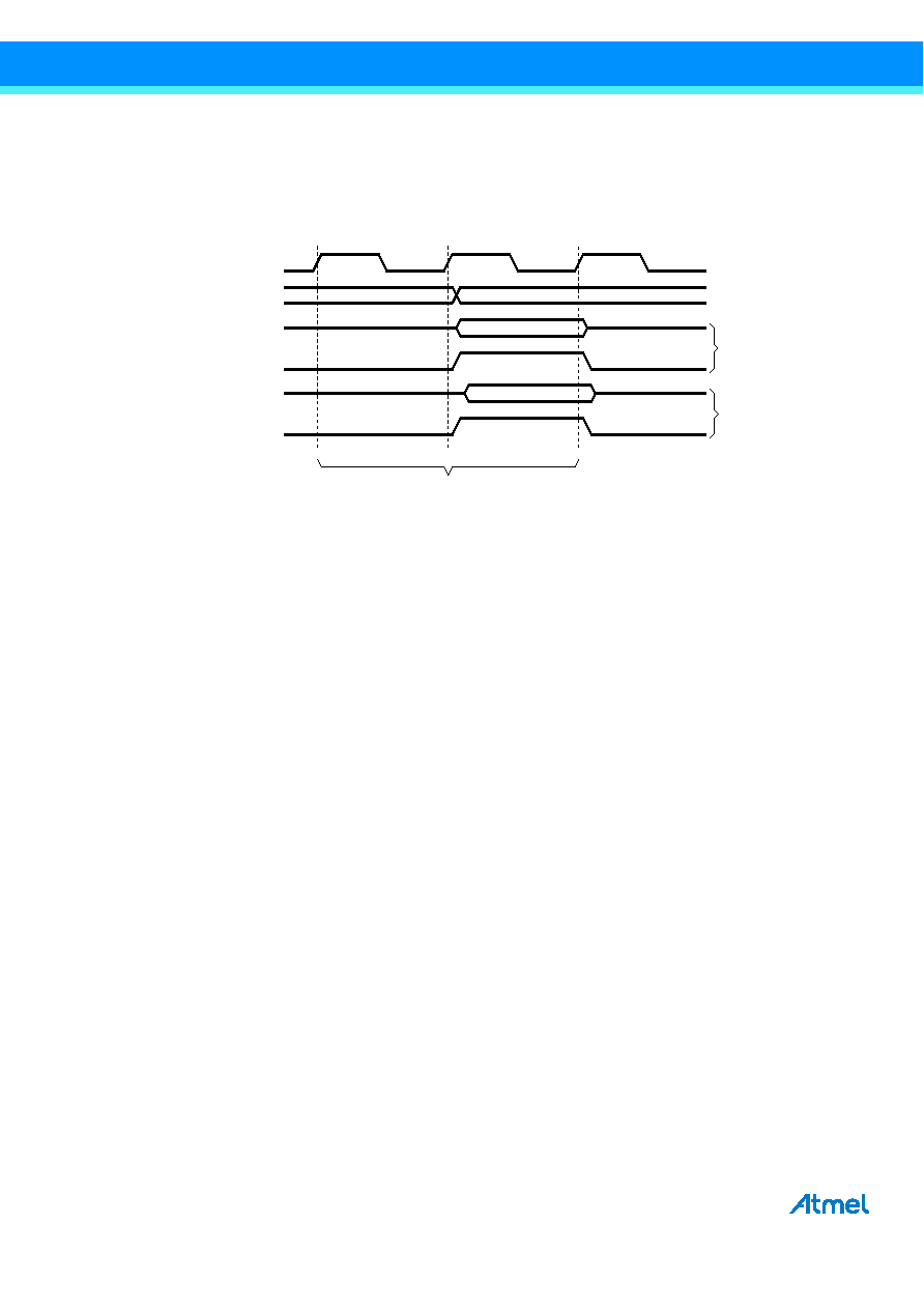
8.3.1
Data Memory Access Times
This section describes the general access timing concepts for internal memory access. The internal data SRAM access is
Figure 8-4. On-chip Data SRAM Access Cycles
8.4
EEPROM Data Memory
The Atmel ATmega48PA/88PA/168PA contains 256/512/512 bytes of data EEPROM memory. It is organized as a separate
data space, in which single bytes can be read and written. The EEPROM has an endurance of at least 100,000 write/erase
cycles. The access between the EEPROM and the CPU is described in the following, specifying the EEPROM address
registers, the EEPROM data register, and the EEPROM control register.
Section 28. “Memory Programming” on page 251 contains a detailed description on EEPROM programming in SPI or
parallel programming mode.
8.4.1
EEPROM Read/Write Access
The EEPROM access registers are accessible in the I/O space.
The write access time for the EEPROM is given in Table 8-2 on page 22. A self-timing function, however, lets the user
software detect when the next byte can be written. If the user code contains instructions that write the EEPROM, some
precautions must be taken. In heavily filtered power supplies, VCC is likely to rise or fall slowly on power-up/down. This
causes the device for some period of time to run at a voltage lower than specified as minimum for the clock frequency used.
See Section 8.4.2 “Preventing EEPROM Corruption” on page 19 for details on how to avoid problems in these situations.
In order to prevent unintentional EEPROM writes, a specific write procedure must be followed. Refer to the description of the
EEPROM Control Register for details on this.
When the EEPROM is read, the CPU is halted for four clock cycles before the next instruction is executed. When the
EEPROM is written, the CPU is halted for two clock cycles before the next instruction is executed.
clk
CPU
T1
Data
RD
WR
Address valid
Compute Address
Next Instruction
Write
Read
Memory Access Instruction
Address
T2
T3
相关PDF资料 |
PDF描述 |
|---|---|
| MB9AF311MPMC | 32-BIT, FLASH, 40 MHz, RISC MICROCONTROLLER, PQFP80 |
| MSP430G2152IRSA16 | 16-BIT, FLASH, 16 MHz, RISC MICROCONTROLLER, PQCC16 |
| M37704E2EFP | 16-BIT, OTPROM, 16 MHz, MICROCONTROLLER, PQFP80 |
| MSM65544-JS | 8-BIT, MROM, 10 MHz, MICROCONTROLLER, PQCC68 |
| MSM65516SS | 8-BIT, MROM, 10 MHz, MICROCONTROLLER, PDIP64 |
相关代理商/技术参数 |
参数描述 |
|---|---|
| MB9AF312KPMC1-G-JNE2 | 功能描述:ARM? Cortex?-M3 FM3 MB9A310K Microcontroller IC 32-Bit 40MHz 160KB (160K x 8) FLASH 52-LQFP (10x10) 制造商:cypress semiconductor corp 系列:FM3 MB9A310K 包装:托盘 零件状态:有效 核心处理器:ARM? Cortex?-M3 核心尺寸:32-位 速度:40MHz 连接性:CSIO,I2C,LIN,UART/USART,USB 外设:DMA,LVD,POR,PWM,WDT I/O 数:36 程序存储容量:160KB(160K x 8) 程序存储器类型:闪存 EEPROM 容量:- RAM 容量:16K x 8 电压 - 电源(Vcc/Vdd):2.7 V ~ 5.5 V 数据转换器:A/D 8x12b 振荡器类型:内部 工作温度:-40°C ~ 105°C(TA) 封装/外壳:52-LQFP 供应商器件封装:52-LQFP(10x10) 标准包装:160 |
| MB9AF312KPMC-ES-E1 | 制造商:FUJITSU 功能描述: |
| MB9AF312KPMC-G-JNE1 | 制造商:FUJITSU 功能描述: |
| MB9AF312KPMC-G-JNE2 | 功能描述:ARM? Cortex?-M3 FM3 MB9A310K Microcontroller IC 32-Bit 40MHz 160KB (160K x 8) FLASH 48-LQFP (7x7) 制造商:cypress semiconductor corp 系列:FM3 MB9A310K 包装:托盘 零件状态:有效 核心处理器:ARM? Cortex?-M3 核心尺寸:32-位 速度:40MHz 连接性:CSIO,I2C,LIN,UART/USART,USB 外设:DMA,LVD,POR,PWM,WDT I/O 数:36 程序存储容量:160KB(160K x 8) 程序存储器类型:闪存 EEPROM 容量:- RAM 容量:16K x 8 电压 - 电源(Vcc/Vdd):2.7 V ~ 5.5 V 数据转换器:A/D 8x12b 振荡器类型:内部 工作温度:-40°C ~ 105°C(TA) 封装/外壳:48-LQFP 供应商器件封装:48-LQFP(7x7) 标准包装:250 |
| MB9AF312KQN-ES-AWE2 | 制造商:FUJITSU 功能描述: |
发布紧急采购,3分钟左右您将得到回复。