- 您现在的位置:买卖IC网 > PDF目录69024 > MB9BF416TBGL (FUJITSU LTD) 32-BIT, FLASH, RISC MICROCONTROLLER, PBGA192 PDF资料下载
参数资料
| 型号: | MB9BF416TBGL |
| 厂商: | FUJITSU LTD |
| 元件分类: | 微控制器/微处理器 |
| 英文描述: | 32-BIT, FLASH, RISC MICROCONTROLLER, PBGA192 |
| 封装: | 12 X 12 MM, 1.45 MM HEIGHT, 0.80 MM PITCH, LEAD FREE, PLASTIC, FBGA-192 |
| 文件页数: | 9/116页 |
| 文件大小: | 1064K |
| 代理商: | MB9BF416TBGL |
第1页第2页第3页第4页第5页第6页第7页第8页当前第9页第10页第11页第12页第13页第14页第15页第16页第17页第18页第19页第20页第21页第22页第23页第24页第25页第26页第27页第28页第29页第30页第31页第32页第33页第34页第35页第36页第37页第38页第39页第40页第41页第42页第43页第44页第45页第46页第47页第48页第49页第50页第51页第52页第53页第54页第55页第56页第57页第58页第59页第60页第61页第62页第63页第64页第65页第66页第67页第68页第69页第70页第71页第72页第73页第74页第75页第76页第77页第78页第79页第80页第81页第82页第83页第84页第85页第86页第87页第88页第89页第90页第91页第92页第93页第94页第95页第96页第97页第98页第99页第100页第101页第102页第103页第104页第105页第106页第107页第108页第109页第110页第111页第112页第113页第114页第115页第116页
106
MB9B410T Series
FUJITSU SEMICONDUCTOR CONFIDENTIAL
r1.0
DS706-00018-0v01-E
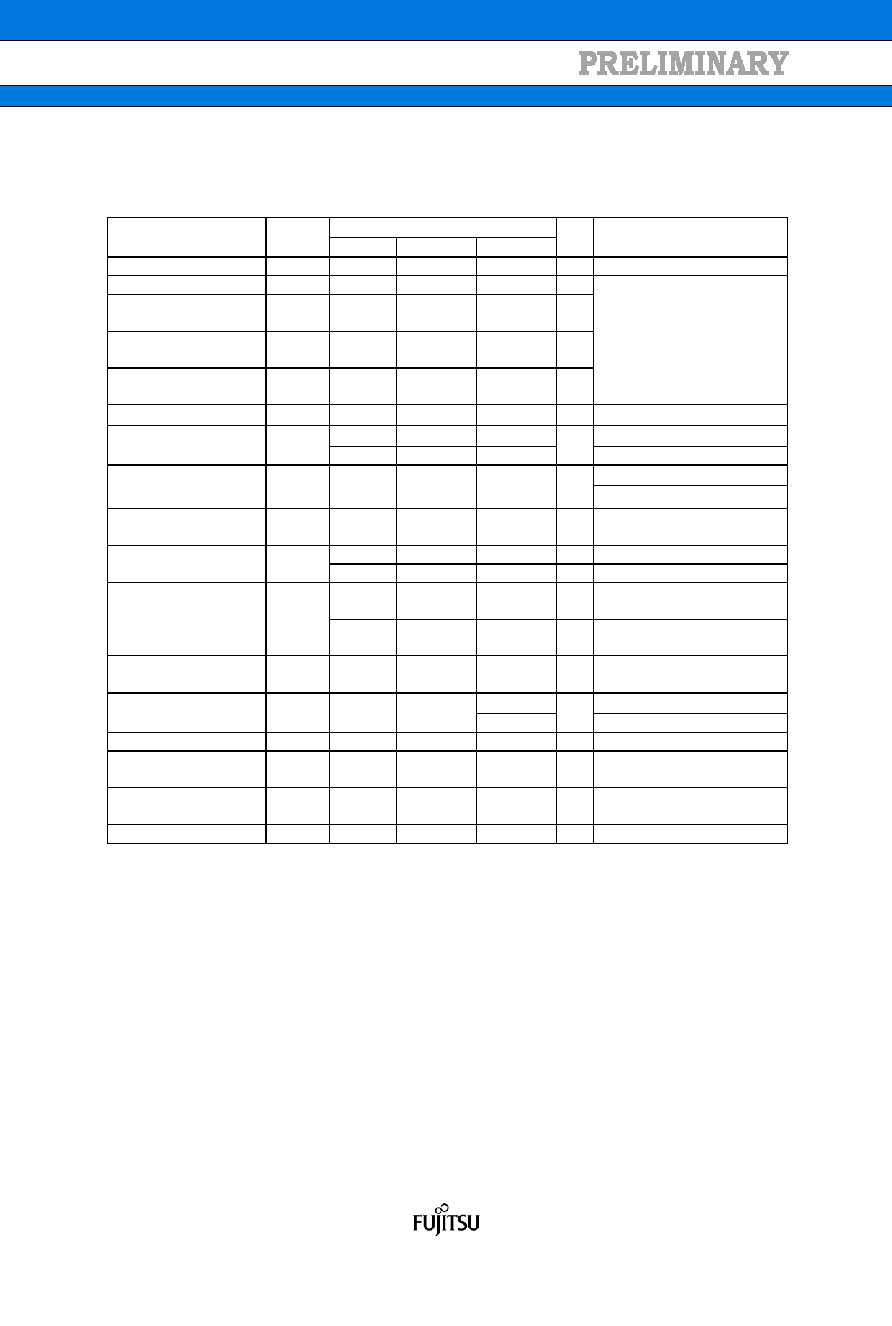
12bit A/D Converter
·
Electrical characteristics for the A/D converter.( Preliminary value)
(Vcc = AVcc = 2.7V to 5.5V, Vss = AVss = 0V, Ta = - 40
°C to + 85°C)
Value
Parameter
Pin
name
Min
Typ
Max
Unit
Remarks
Resolution
-
12
bit
Linearity error
-
- 4.5
-
+ 4.5
LSB
Differential linearity
error
-
-2.5
-
+ 2.5
LSB
Zero transition voltage
AN0 to
AN31
- 20
-
+ 20
mV
Full transition voltage
AN0 to
AN31
- 20
-
+ 20
mV
AVRH = 2.7V to 5.5V
Conversion time
-
1.0*1
-
μs AVcc
≥ 4.5V
*2
-
AVcc
≥ 4.5V
Sampling time
Ts
*2
-
ns
AVcc < 4.5V
AVcc
≥ 4.5V
Compare clock cycle*3
Tcck
50
-
10000
ns
AVcc < 4.5V
State transition time to
operation permission
Tstt
1.0
-
μs
-
0.47
0.62
mA A/D 1unit operation
Power supply current
(analog + digital)
AVCC
-
0.01
TBD
μA When A/D stop (1unit)
-
1.1
1.96
mA
A/D 1unit operation
AVRH=5.5V
Reference power supply
current
(between AVRH to
AVSS)
AVRH
-
0.01
1.6
μA When A/D stop (1unit)
Analog input capacity
Cin
-
12.9
pF
2
AVcc
≥ 4.5V
Analog input resistance
Rin
-
3.8
k
AVcc < 4.5V
Interchannel disparity
-
4
LSB
Analog port input
current
AN0 to
AN31
-
5
μA
Analog input voltage
AN0 to
AN31
AVSS
-
AVRH
V
Reference voltage
AVRH
AVSS
-
AVCC
V
*1: Conversion time is the value of sampling time(Ts) + compare time(Tc).
The condition of the minimum conversion time is when HCLK=40MHz, the value of sampling time: 0.3μs,
the value of sampling time: 700ns (AVcc
≥ 4.5V).
Ensure that it satisfies the value of sampling time(Ts) and compare clock cycle (Tcck).
For setting*4 of sampling time and compare clock cycle, see chapter "Chapter:12-bit A/D Converter" in
"FM3 FAMILY MB9Axxx/MB9Bxxx Series PERIPHERAL MANUAL".
*2: A necessary sampling time changes by external impedance.
Ensure that it set the sampling time to satisfy (Equation 1).
*3: Compare time (Tc) is the value of (Equation 2).
*4: The register setting of the A/D Converter is reflected by the timing of the APB bus clock.
Sampling clock and compare clock are set with the base clock (HCLK).
About the APB bus number which A/D Converter is connected to, see chapter " BLOCK DIAGRAM"
in this data sheet.
相关PDF资料 |
PDF描述 |
|---|---|
| MC12430FA | 800 MHz, OTHER CLOCK GENERATOR, PQFP32 |
| MC13214R2 | SPECIALTY MICROPROCESSOR CIRCUIT, BGA71 |
| MC13224VR2 | SPECIALTY MICROPROCESSOR CIRCUIT, PBGA99 |
| MC13226V | SPECIALTY MICROPROCESSOR CIRCUIT, PBGA99 |
| MC13226VR2 | SPECIALTY MICROPROCESSOR CIRCUIT, PBGA99 |
相关代理商/技术参数 |
参数描述 |
|---|---|
| MB9BF466LPMC1-G-JNE2 | 功能描述:IC MCU 32BIT 544KB FLASH 64LQFP 制造商:cypress semiconductor corp 系列:FM4 MB9B460L 包装:托盘 零件状态:在售 核心处理器:ARM? Cortex?-M4F 核心尺寸:32-位 速度:160MHz 连接性:CAN,CSIO,I2C,LIN,UART/USART 外设:DMA,LVD,POR,PWM,WDT I/O 数:48 程序存储容量:544KB(544K x 8) 程序存储器类型:闪存 EEPROM 容量:- RAM 容量:64K x 8 电压 - 电源(Vcc/Vdd):2.7 V ~ 5.5 V 数据转换器:A/D 15x12b,A/D 2x10b 振荡器类型:内部 工作温度:-40°C ~ 125°C(TA) 封装/外壳:64-LQFP 供应商器件封装:64-LQFP(10x10) 标准包装:160 |
| MB9BF500 | 制造商:FUJITSU 制造商全称:Fujitsu Component Limited. 功能描述:32-bit MCUs with ARM Cortex-M3 Core |
| MB9BF504NBPMC-G-JNE2 | 制造商:FUJITSU 功能描述: |
| MB9BF504NPMC-G-JNE1 | 功能描述:IC MCU 32BIT 256KB FLASH 100LQFP RoHS:是 类别:集成电路 (IC) >> 嵌入式 - 微控制器, 系列:FM3 MB9B500 产品培训模块:MCU Product Line Introduction XMEGA Introduction AVR XMEGA USB Connectivity 标准包装:90 系列:AVR® XMEGA 核心处理器:AVR 芯体尺寸:8/16-位 速度:32MHz 连通性:I²C,IrDA,SPI,UART/USART 外围设备:欠压检测/复位,DMA,POR,PWM,WDT 输入/输出数:50 程序存储器容量:192KB(96K x 16) 程序存储器类型:闪存 EEPROM 大小:4K x 8 RAM 容量:16K x 8 电压 - 电源 (Vcc/Vdd):1.6 V ~ 3.6 V 数据转换器:A/D 16x12b; D/A 2x12b 振荡器型:内部 工作温度:-40°C ~ 85°C 封装/外壳:64-TQFP 包装:托盘 配用:ATSTK600-RC14-ND - STK600 SOCKET/ADAPTER 64TQFPATSTK600-TQFP64-ND - STK600 SOCKET/ADAPTER 64-TQFPATAVRONEKIT-ND - KIT AVR/AVR32 DEBUGGER/PROGRMMRATAVRISP2-ND - PROGRAMMER AVR IN SYSTEM |
| MB9BF504RPMC | 制造商:FUJITSU 制造商全称:Fujitsu Component Limited. 功能描述:Family of 32-bit MCUs |
发布紧急采购,3分钟左右您将得到回复。