- 您现在的位置:买卖IC网 > PDF目录98011 > MBT3906DW1T2 (ON SEMICONDUCTOR) 200 mA, 40 V, 2 CHANNEL, PNP, Si, SMALL SIGNAL TRANSISTOR PDF资料下载
参数资料
| 型号: | MBT3906DW1T2 |
| 厂商: | ON SEMICONDUCTOR |
| 元件分类: | 小信号晶体管 |
| 英文描述: | 200 mA, 40 V, 2 CHANNEL, PNP, Si, SMALL SIGNAL TRANSISTOR |
| 封装: | SC-88, 6 PIN |
| 文件页数: | 8/30页 |
| 文件大小: | 471K |
| 代理商: | MBT3906DW1T2 |
第1页第2页第3页第4页第5页第6页第7页当前第8页第9页第10页第11页第12页第13页第14页第15页第16页第17页第18页第19页第20页第21页第22页第23页第24页第25页第26页第27页第28页第29页第30页
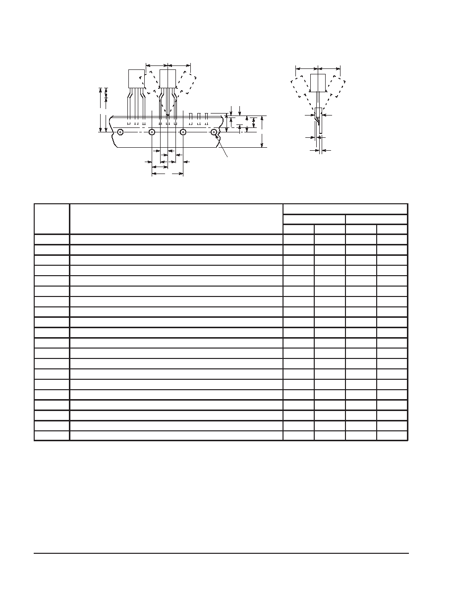
Packaging Specifications
6–6
Motorola Small–Signal Transistors, FETs and Diodes Device Data
TO–92 EIA RADIAL TAPE IN FAN FOLD BOX OR ON REEL
H2A
H
F1
F2
P2
P1
P
D
W
W1
L1
W2
H2B
T1
T
T2
H4 H5
H1
Figure 1. Device Positioning on Tape
L
Specification
Inches
Millimeter
Symbol
Item
Min
Max
Min
Max
D
Tape Feedhole Diameter
0.1496
0.1653
3.8
4.2
D2
Component Lead Thickness Dimension
0.015
0.020
0.38
0.51
F1, F2
Component Lead Pitch
0.0945
0.110
2.4
2.8
H
Bottom of Component to Seating Plane
.059
.156
1.5
4.0
H1
Feedhole Location
0.3346
0.3741
8.5
9.5
H2A
Deflection Left or Right
0
0.039
0
1.0
H2B
Deflection Front or Rear
0
0.051
0
1.0
H4
Feedhole to Bottom of Component
0.7086
0.768
18
19.5
H5
Feedhole to Seating Plane
0.610
0.649
15.5
16.5
L
Defective Unit Clipped Dimension
0.3346
0.433
8.5
11
L1
Lead Wire Enclosure
0.09842
—
2.5
—
P
Feedhole Pitch
0.4921
0.5079
12.5
12.9
P1
Feedhole Center to Center Lead
0.2342
0.2658
5.95
6.75
P2
First Lead Spacing Dimension
0.1397
0.1556
3.55
3.95
T
Adhesive Tape Thickness
0.06
0.08
0.15
0.20
T1
Overall Taped Package Thickness
—
0.0567
—
1.44
T2
Carrier Strip Thickness
0.014
0.027
0.35
0.65
W
Carrier Strip Width
0.6889
0.7481
17.5
19
W1
Adhesive Tape Width
0.2165
0.2841
5.5
6.3
W2
Adhesive Tape Position
.0059
0.01968
.15
0.5
NOTES:
1. Maximum alignment deviation between leads not to be greater than 0.2 mm.
2. Defective components shall be clipped from the carrier tape such that the remaining protrusion (L) does not exceed a maximum of 11 mm.
3. Component lead to tape adhesion must meet the pull test requirements established in Figures 5, 6 and 7.
4. Maximum non–cumulative variation between tape feed holes shall not exceed 1 mm in 20 pitches.
5. Holddown tape not to extend beyond the edge(s) of carrier tape and there shall be no exposure of adhesive.
6. No more than 1 consecutive missing component is permitted.
7. A tape trailer and leader, having at least three feed holes is required before the first and after the last component.
8. Splices will not interfere with the sprocket feed holes.
相关PDF资料 |
PDF描述 |
|---|---|
| MBT3904DW1T2 | 200 mA, 40 V, 2 CHANNEL, NPN, Si, SMALL SIGNAL TRANSISTOR |
| MBT3906DW1T3 | 200 mA, 40 V, 2 CHANNEL, PNP, Si, SMALL SIGNAL TRANSISTOR |
| MBT3946DW1T1 | 200 mA, 40 V, 2 CHANNEL, NPN AND PNP, Si, SMALL SIGNAL TRANSISTOR |
| MBT3906DW1T1 | 200 mA, 40 V, 2 CHANNEL, PNP, Si, SMALL SIGNAL TRANSISTOR |
| MC-10118BF1-ENY-A | SPECIALTY MICROPROCESSOR CIRCUIT, PBGA481 |
相关代理商/技术参数 |
参数描述 |
|---|---|
| MBT3906DW1T2G | 制造商:ON Semiconductor 功能描述:SS SC88 GP XSTR PNP 40V - Tape and Reel 制造商:ON Semiconductor 功能描述:Dual PNP Bipolar Transistor 制造商:ON Semiconductor 功能描述:REEL - SS SC88 GP XSTR PNP 40V |
| MBT3906DW1T3 | 制造商:Rochester Electronics LLC 功能描述:- Tape and Reel 制造商:ON Semiconductor 功能描述: |
| MBT3946DW | 制造商:WEITRON 制造商全称:Weitron Technology 功能描述:Dual General Purpose Transistor NPN+PNP Silicon |
| MBT3946DW1T1 | 功能描述:两极晶体管 - BJT 200mA 40V Dual RoHS:否 制造商:STMicroelectronics 配置: 晶体管极性:PNP 集电极—基极电压 VCBO: 集电极—发射极最大电压 VCEO:- 40 V 发射极 - 基极电压 VEBO:- 6 V 集电极—射极饱和电压: 最大直流电集电极电流: 增益带宽产品fT: 直流集电极/Base Gain hfe Min:100 A 最大工作温度: 安装风格:SMD/SMT 封装 / 箱体:PowerFLAT 2 x 2 |
| MBT3946DW1T1G | 功能描述:两极晶体管 - BJT 200mA 40V Dual Complementary RoHS:否 制造商:STMicroelectronics 配置: 晶体管极性:PNP 集电极—基极电压 VCBO: 集电极—发射极最大电压 VCEO:- 40 V 发射极 - 基极电压 VEBO:- 6 V 集电极—射极饱和电压: 最大直流电集电极电流: 增益带宽产品fT: 直流集电极/Base Gain hfe Min:100 A 最大工作温度: 安装风格:SMD/SMT 封装 / 箱体:PowerFLAT 2 x 2 |
发布紧急采购,3分钟左右您将得到回复。