参数资料
| 型号: | MC100E196FNR2G |
| 厂商: | ON Semiconductor |
| 文件页数: | 10/12页 |
| 文件大小: | 0K |
| 描述: | IC DELAY LINE 128TAP 28-PLCC |
| 产品变化通告: | Dimensional change 21/Oct/2008 |
| 标准包装: | 500 |
| 系列: | 100E |
| 标片/步级数: | 128 |
| 功能: | 可编程 |
| 延迟到第一抽头: | 1.39ns |
| 接头增量: | 20ps |
| 可用的总延迟: | 1.39ns ~ 3.63ns |
| 独立延迟数: | 1 |
| 电源电压: | 4.2 V ~ 5.7 V |
| 工作温度: | 0°C ~ 85°C |
| 安装类型: | 表面贴装 |
| 封装/外壳: | 28-LCC(J 形引线) |
| 供应商设备封装: | 28-PLCC(11.51x11.51) |
| 包装: | 带卷 (TR) |
MC10E196, MC100E196
http://onsemi.com
7
FTUNE VOLTAGE (V)
140
120
100
80
60
40
20
0
4.5
3.5
2.5
1.5
0.5
PROP
AGA
TION
DELA
Y
(ps)
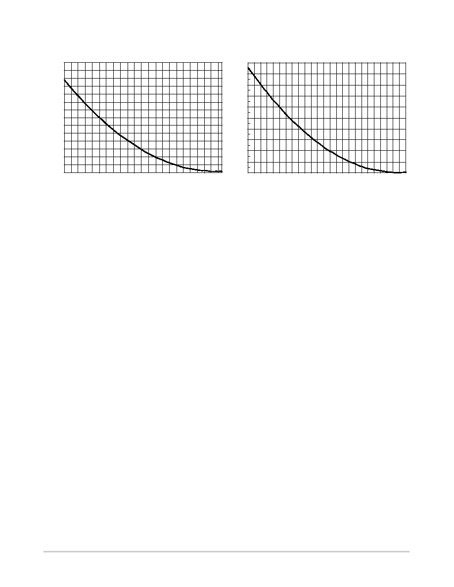
Propagation Delay versus FTUNE Voltage
(100E196)
FTUNE VOLTAGE (V)
100
90
80
70
60
50
40
30
20
10
0
5
4
3
2
1
0
PROP
AGA
TION
DELA
Y
(ps)
Propagation Delay versus FTUNE Voltage
(10E196)
ANALOG INPUT CHARACTERISTICS
FTUNE = VCC to VEE
USING THE FTUNE ANALOG INPUT
The analog FTUNE pin on the E196 device is intended to
add more delay in a tunable gate to enhance the 20 ps
resolution capabilities of the fully digital E195. The level of
resolution obtained is dependent on the number of
increments applied to the appropriate range on the FTUNE
pin.
To provide this further level of resolution (See Logic
Diagram), the FTUNE pin must be capable of adjusting the
additional delay finer than the 20 ps digital resolution. From
the provided graphs one sees that this requirement is easily
achieved as over the entire FTUNE voltage range a 100 ps
additional delay can be achieved. This extra analog range
ensures that the FTUNE pin will be capable even under
worst case conditions of covering the digital resolution.
Typically the analog input will be driven by an external DAC
to provide a digital control with very fine analog output
steps. The final resolution of the device will be dependent on
the width of the DAC chosen.
To determine the voltage range necessary for the FTUNE
input, the graphs provided should be used. As an example if
a tuning range of 40 ps is selected to cover worst case
conditions and ensure coverage of the digital range, from the
100E196 graph a voltage range of 3.25 V to 4.0 V would
be necessary on the FTUNE pin. Obviously there are
numerous voltage ranges which can be used to cover a given
delay range, users are given the flexibility to determine
which one best fits their designs.
Cascading Multiple E196’s
To increase the programmable range of the E196 internal
cascade circuitry has been included. This circuitry allows for
the cascading of multiple E196’s without the need for any
external gating. Furthermore this capability requires only
one more address line per added E196. Obviously cascading
multiple PDC’s will result in a larger programmable range,
however, this increase is at the expense of a longer minimum
delay.
Figure 3 illustrates the interconnect scheme for
cascading two E196’s. As can be seen, this scheme can
easily be expanded for larger E196 chains. The D7 input of
the E196 is the cascade control pin. With the interconnect
scheme of Figure 3 when D7 is asserted it signals the need
for a larger programmable range than is achievable with a
single device.
An expansion of the latch section of the block diagram is
pictured below. Use of this diagram will simplify the
explanation of how the cascade circuitry works. When D7
of chip #1 above is low the cascade output will also be low
while the cascade bar output will be a logical high. In this
condition the SET MIN pin of chip #2 will be asserted and
thus all of the latches of chip #2 will be reset and the device
will be set at its minimum delay. Since the RESET and SET
inputs of the latches are overriding any changes on the
A0A6 address bus will not affect the operation of chip #2.
Chip #1 on the other hand will have both SET MIN and
SET MAX de-asserted so that its delay will be controlled
entirely by the address bus A0A6. If the delay needed is
greater than can be achieved with 31.75 gate delays
(1111111 on the A0A6 address bus) D7 will be asserted to
signal the need to cascade the delay to the next E196 device.
When D7 is asserted the SET MIN pin of chip #2 will be
de-asserted and the delay will be controlled by the A0A6
address bus. Chip #1 on the other hand will have its SET
MAX pin asserted resulting in the device delay to be
independent of the A0A6 address bus.
相关PDF资料 |
PDF描述 |
|---|---|
| MC100E195FNR2G | IC DELAY LINE 128TAP 28-PLCC |
| VI-2WK-MX-B1 | CONVERTER MOD DC/DC 40V 75W |
| SY55856UHG TR | IC DELAY LINE 7TAP 32-TQFP |
| M83723/76R18086 | CONN PLUG 8POS STRAIGHT W/PINS |
| SY89296UMG | IC DELAY LINE 1024TAP 32-MLF |
相关代理商/技术参数 |
参数描述 |
|---|---|
| MC100E210 | 制造商:ONSEMI 制造商全称:ON Semiconductor 功能描述:5V ECL Dual 1:4, 1:5 Differential Fanout Buffer |
| MC100E210FN | 功能描述:时钟缓冲器 5V ECL Dual 1:4 1:5 RoHS:否 制造商:Texas Instruments 输出端数量:5 最大输入频率:40 MHz 传播延迟(最大值): 电源电压-最大:3.45 V 电源电压-最小:2.375 V 最大功率耗散: 最大工作温度:+ 85 C 最小工作温度:- 40 C 封装 / 箱体:LLP-24 封装:Reel |
| MC100E210FNG | 功能描述:时钟缓冲器 5V ECL Dual 1:4 1:5 Diff Fanout Buffer RoHS:否 制造商:Texas Instruments 输出端数量:5 最大输入频率:40 MHz 传播延迟(最大值): 电源电压-最大:3.45 V 电源电压-最小:2.375 V 最大功率耗散: 最大工作温度:+ 85 C 最小工作温度:- 40 C 封装 / 箱体:LLP-24 封装:Reel |
| MC100E210FNR2 | 功能描述:时钟缓冲器 5V ECL Dual 1:4 1:5 RoHS:否 制造商:Texas Instruments 输出端数量:5 最大输入频率:40 MHz 传播延迟(最大值): 电源电压-最大:3.45 V 电源电压-最小:2.375 V 最大功率耗散: 最大工作温度:+ 85 C 最小工作温度:- 40 C 封装 / 箱体:LLP-24 封装:Reel |
| MC100E210FNR2G | 功能描述:时钟缓冲器 5V ECL Dual 1:4 1:5 Diff Fanout Buffer RoHS:否 制造商:Texas Instruments 输出端数量:5 最大输入频率:40 MHz 传播延迟(最大值): 电源电压-最大:3.45 V 电源电压-最小:2.375 V 最大功率耗散: 最大工作温度:+ 85 C 最小工作温度:- 40 C 封装 / 箱体:LLP-24 封装:Reel |
发布紧急采购,3分钟左右您将得到回复。