参数资料
| 型号: | MC100E196FNR2G |
| 厂商: | ON Semiconductor |
| 文件页数: | 9/12页 |
| 文件大小: | 0K |
| 描述: | IC DELAY LINE 128TAP 28-PLCC |
| 产品变化通告: | Dimensional change 21/Oct/2008 |
| 标准包装: | 500 |
| 系列: | 100E |
| 标片/步级数: | 128 |
| 功能: | 可编程 |
| 延迟到第一抽头: | 1.39ns |
| 接头增量: | 20ps |
| 可用的总延迟: | 1.39ns ~ 3.63ns |
| 独立延迟数: | 1 |
| 电源电压: | 4.2 V ~ 5.7 V |
| 工作温度: | 0°C ~ 85°C |
| 安装类型: | 表面贴装 |
| 封装/外壳: | 28-LCC(J 形引线) |
| 供应商设备封装: | 28-PLCC(11.51x11.51) |
| 包装: | 带卷 (TR) |
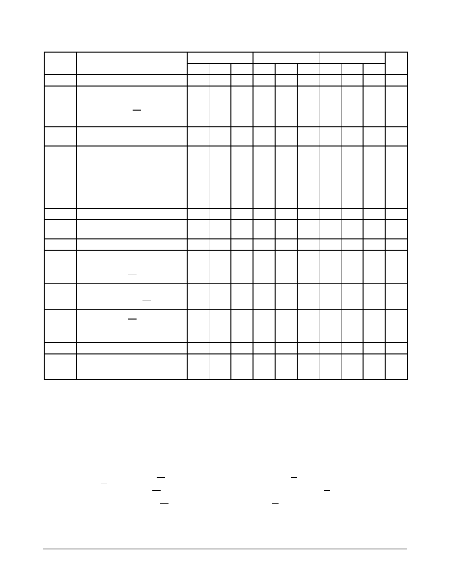
MC10E196, MC100E196
http://onsemi.com
6
Symbol
Characteristic
0°C
25°C
85°C
Unit
Min
Typ
Max
Min
Typ
Max
Min
Typ
Max
fMAX
Maximum Toggle Frequency
>1.0
GHz
tPLH
tPHL
Propagation Delay
IN to Q; Tap = 0
IN to Q; Tap = 127
EN to Q; Tap = 0
D7 to CASCADE
1210
3320
1250
300
1360
3570
1450
450
1510
3820
1650
700
1240
3380
1275
300
1390
3630
1475
450
1540
3880
1675
700
1440
3920
1350
300
1590
4270
1650
450
1765
4720
1950
700
ps
tRANGE
Programmable Range
tPD (max) tPD (min)
2000
2175
2050
2240
2375
2580
ps
Dt
Step Delay (Note 14)
D0 High
D1 High
D2 High
D3 High
D4 High
D5 High
D6 High
55
115
250
505
1000
17
34
68
136
272
544
1088
105
180
325
620
1190
55
115
250
515
1030
17.5
35
70
140
280
560
1120
105
180
325
620
1220
65
140
305
620
1240
21
42
84
168
336
672
1344
120
205
380
740
1450
ps
Lin
Linearity (Note 15)
D1
D0
D1
D0
D1
D0
tSKEW
Duty Cycle Skew
±30
ps
tJITTER
Random Clock Jitter (RMS)
< 5
ps
ts
Setup Time
D to LEN
D to IN (Note 17)
EN to IN (Note 18)
200
800
200
0
200
800
200
0
200
800
200
0
ps
th
Hold Time
LEN to D
IN to EN (Note 19)
500
0
250
500
0
250
500
0
250
ps
tR
Release Time
EN to IN (Note 20)
SET MAX to LEN
SET MIN to LEN
300
800
300
800
300
800
ps
tjit
Random Clock Jitter (RMS)
< 5
ps
tr
tf
Output Rise/Fall Time
2080% (Q)
2080% (CASCADE)
125
300
225
450
325
650
125
300
225
450
325
650
125
300
225
450
325
650
ps
NOTE: Device will meet the specifications after thermal equilibrium has been established when mounted in a test socket or printed circuit
board with maintained transverse airflow greater than 500 lfpm. Electrical parameters are guaranteed only over the declared
operating temperature range. Functional operation of the device exceeding these conditions is not implied. Device specification limit
values are applied individually under normal operating conditions and not valid simultaneously.
13.10 Series: VEE can vary 0.46 V / +0.06 V.
100 Series: VEE can vary 0.46 V / +0.8 V.
14.Specification limits represent the amount of delay added with the assertion of each individual delay control pin. The various combinations
of asserted delay control inputs will typically realize D0 resolution steps across the specified programmable range.
15.The linearity specification guarantees to which delay control input the programmable steps will be monotonic (i.e. increasing delay steps for
increasing binary counts on the control inputs Dn). Typically the device will be monotonic to the D0 input, however under worst case conditions
and process variation, delays could decrease slightly with increasing binary counts when the D0 input is the LSB. With the D1 input as the
LSB the device is guaranteed to be monotonic over all specified environmental conditions and process variation.
16.Duty cycle skew guaranteed only for differential operation measured from the cross point of the input to the cross point of the output.
17.This setup time defines the amount of time prior to the input signal the delay tap of the device must be set.
18.This setup time is the minimum time that EN must be asserted prior to the next transition of IN/IN to prevent an output response greater than
±75 mV to that IN/IN transition.
19.This hold time is the minimum time that EN must remain asserted after a negative going IN or positive going IN to prevent an output response
greater than ±75 mV to that IN/IN transition.
20.This release time is the minimum time that EN must be deasserted prior to the next IN/IN transition to ensure an output response that meets
the specified IN to Q propagation delay and transition times.
相关PDF资料 |
PDF描述 |
|---|---|
| MC100E195FNR2G | IC DELAY LINE 128TAP 28-PLCC |
| VI-2WK-MX-B1 | CONVERTER MOD DC/DC 40V 75W |
| SY55856UHG TR | IC DELAY LINE 7TAP 32-TQFP |
| M83723/76R18086 | CONN PLUG 8POS STRAIGHT W/PINS |
| SY89296UMG | IC DELAY LINE 1024TAP 32-MLF |
相关代理商/技术参数 |
参数描述 |
|---|---|
| MC100E210 | 制造商:ONSEMI 制造商全称:ON Semiconductor 功能描述:5V ECL Dual 1:4, 1:5 Differential Fanout Buffer |
| MC100E210FN | 功能描述:时钟缓冲器 5V ECL Dual 1:4 1:5 RoHS:否 制造商:Texas Instruments 输出端数量:5 最大输入频率:40 MHz 传播延迟(最大值): 电源电压-最大:3.45 V 电源电压-最小:2.375 V 最大功率耗散: 最大工作温度:+ 85 C 最小工作温度:- 40 C 封装 / 箱体:LLP-24 封装:Reel |
| MC100E210FNG | 功能描述:时钟缓冲器 5V ECL Dual 1:4 1:5 Diff Fanout Buffer RoHS:否 制造商:Texas Instruments 输出端数量:5 最大输入频率:40 MHz 传播延迟(最大值): 电源电压-最大:3.45 V 电源电压-最小:2.375 V 最大功率耗散: 最大工作温度:+ 85 C 最小工作温度:- 40 C 封装 / 箱体:LLP-24 封装:Reel |
| MC100E210FNR2 | 功能描述:时钟缓冲器 5V ECL Dual 1:4 1:5 RoHS:否 制造商:Texas Instruments 输出端数量:5 最大输入频率:40 MHz 传播延迟(最大值): 电源电压-最大:3.45 V 电源电压-最小:2.375 V 最大功率耗散: 最大工作温度:+ 85 C 最小工作温度:- 40 C 封装 / 箱体:LLP-24 封装:Reel |
| MC100E210FNR2G | 功能描述:时钟缓冲器 5V ECL Dual 1:4 1:5 Diff Fanout Buffer RoHS:否 制造商:Texas Instruments 输出端数量:5 最大输入频率:40 MHz 传播延迟(最大值): 电源电压-最大:3.45 V 电源电压-最小:2.375 V 最大功率耗散: 最大工作温度:+ 85 C 最小工作温度:- 40 C 封装 / 箱体:LLP-24 封装:Reel |
发布紧急采购,3分钟左右您将得到回复。