- 您现在的位置:买卖IC网 > PDF目录2093 > MC100ES6014EJR2 (IDT, Integrated Device Technology Inc)IC CLOCK BUFFER MUX 2:5 20-TSSOP PDF资料下载
参数资料
| 型号: | MC100ES6014EJR2 |
| 厂商: | IDT, Integrated Device Technology Inc |
| 文件页数: | 3/8页 |
| 文件大小: | 0K |
| 描述: | IC CLOCK BUFFER MUX 2:5 20-TSSOP |
| 标准包装: | 2,500 |
| 系列: | 100ES |
| 类型: | 扇出缓冲器(分配),多路复用器 |
| 电路数: | 1 |
| 比率 - 输入:输出: | 2:5 |
| 差分 - 输入:输出: | 是/是 |
| 输入: | ECL,HSTL,LVDS,PECL |
| 输出: | ECL,PECL |
| 频率 - 最大: | 2GHz |
| 电源电压: | ±2.375 V ~ 3.8 V |
| 工作温度: | -40°C ~ 85°C |
| 安装类型: | 表面贴装 |
| 封装/外壳: | 20-TSSOP(0.173",4.40mm 宽) |
| 供应商设备封装: | 20-TSSOP |
| 包装: | 带卷 (TR) |
MC100ES6014 REVISION 4 DECEMBER 18, 2012
3
2012 Integrated Device Technology, Inc.
MC100ES6014 Data Sheet
2.5 V/3.3 V 1:5 Differential ECL/PECL/HSTL/LVDS Clock Driver
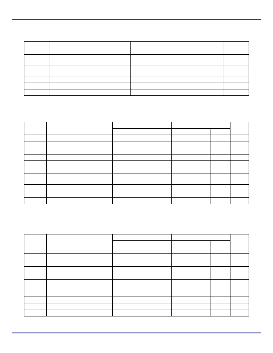
Table 4. Absolute Maximum Ratings(1)
1. Absolute maximum continuous ratings are those maximum values beyond which damage to the device may occur. Exposure to these
conditions or conditions beyond those indicated may adversely affect device reliability. Functional operation at absolute-maximum-rated
conditions is not implied.
Symbol
Characteristic
Conditions
Rating
Units
VSUPPLY
Power Supply Voltage
Difference between VCC & VEE
3.9
V
VIN
Input Voltage
VCC – VEE 3.6 V
VCC + 0.3
VEE – 0.3
V
IOUT
Output Current
Continuous
Surge
50
100
mA
IBB
VBB Sink/Source Current
±0.5
C
TA
Operating Temperature Range
–40 to +85
C
TSTG
Storage Temperature Range
–65 to +150
C
Table 5. DC Characteristics (VCC = 0 V, VEE = –2.5 V ± 5% or VCC = 2.5 V ± 5%, VEE = 0 V)
Symbol
Characteristics
–40°C
0°C to 85°C
Unit
Min
Typ
Max
Min
Typ
Max
IEE
Power Supply Current
30
60
30
60
mA
VOH
Output HIGH Voltage(1)
1. Output termination voltage VTT = 0 V for VCC = 2.5 V operation is supported but the power consumption of the device will increase.
VCC–1250 VCC–990
VCC–800 VCC–1200 VCC–960
VCC–750
mV
VOL
Output LOW Voltage(1)
VCC–2000 VCC–1550 VCC–1150 VCC–1925 VCC–1630 VCC–1200
mV
VoutPP
Output Peak-to-Peak Voltage
200
mV
VIH
Input HIGH Voltage
VCC–1165
VCC–880 VCC–1165
VCC–880
mV
VIL
Input LOW Voltage
VCC–1810
VCC–1475 VCC–1810
VCC–1475
mV
VBB
Output Reference Voltage
IBB = 200 A
VCC–1400
VCC–1200 VCC–1400
VCC–1200
mV
VPP
Differential Input Voltage(2)
2. VPP (DC) is the minimum differential input voltage swing required to maintain device functionality.
0.12
1.3
0.12
1.3
mV
VCMR
Differential Cross Point Voltage(3)
3. VCMR (DC) is the crosspoint of the differential input signal. Functional operation is obtained when the crosspoint is within the VCMR (DC)
range and the input swing lies within the VPP (DC) specification.
VEE+0.2
VCC–1.0
VEE+0.2
VCC–1.0
mV
IIN
Input Current
±150
A
Table 6. DC Characteristics (VCC = 0 V, VEE = –3.8 V to –3.135 V or VCC = 3.135 V to 3.8 V, VEE = 0 V)
Symbol
Characteristics
–40°C
0°C to 85°C
Unit
Min
Typ
Max
Min
Typ
Max
IEE
Power Supply Current
30
60
30
60
mA
VOH
Output HIGH Voltage(1)
1. Output termination voltage VTT = 0 V for VCC = 2.5 V operation is supported but the power consumption of the device will increase.
VCC–1150 VCC–1020 VCC–800 VCC–1200 VCC–970
VCC–750
mV
VOL
Output LOW Voltage(1)
VCC–1950 VCC–1620 VCC–1250 VCC–2000 VCC–1680 VCC–1300
mV
VoutPP
Output Peak-to-Peak Voltage
200
mV
VIH
Input HIGH Voltage
VCC–1165
VCC–880 VCC–1165
VCC–880
mV
VIL
Input LOW Voltage
VCC–1810
VCC–1475 VCC–1810
VCC–1475
mV
VBB
Output Reference Voltage
IBB = 200 A
VCC–1400
VCC–1200 VCC–1400
VCC–1200
mV
VPP
Differential Input Voltage(2)
2. VPP (DC) is the minimum differential input voltage swing required to maintain device functionality.
0.12
1.3
0.12
1.3
V
VCMR
Differential Cross Point Voltage(3)
VEE+0.2
VCC–1.1
VEE+0.2
VCC–1.1
V
IIN
Input Current
±150
A
相关PDF资料 |
PDF描述 |
|---|---|
| MC100ES6039EG | IC CLK GENERATION CHIP 20-SOIC |
| MC100ES6056EG | IC CLOCK MUX 2:1 3GHZ 20-SOIC |
| MC100ES60T23EFR2 | IC XLATOR LV PECL DUAL 8-SOIC |
| MC100ES6130EJ | IC CLOCK BUFFER MUX 2:4 16-TSSOP |
| MC100ES6210KLF | IC CLOCK BUFFER 1:5 3GHZ 32VFQFN |
相关代理商/技术参数 |
参数描述 |
|---|---|
| MC100ES6017DW | 制造商:Integrated Device Technology Inc 功能描述:LINE RCVR 4RX 20SOIC - Rail/Tube |
| MC100ES6017DWR2 | 制造商:Integrated Device Technology Inc 功能描述:LINE RCVR 4RX 20SOIC - Tape and Reel |
| MC100ES6017EG | 功能描述:时钟驱动器及分配 FSL LVPECL Quad Diff Receiver RoHS:否 制造商:Micrel 乘法/除法因子:1:4 输出类型:Differential 最大输出频率:4.2 GHz 电源电压-最大: 电源电压-最小:5 V 最大工作温度:+ 85 C 封装 / 箱体:SOIC-8 封装:Reel |
| MC100ES6017EGR2 | 功能描述:时钟缓冲器 FSL LVPECL Quad Diff Receiver RoHS:否 制造商:Texas Instruments 输出端数量:5 最大输入频率:40 MHz 传播延迟(最大值): 电源电压-最大:3.45 V 电源电压-最小:2.375 V 最大功率耗散: 最大工作温度:+ 85 C 最小工作温度:- 40 C 封装 / 箱体:LLP-24 封装:Reel |
| MC100ES6030DW | 制造商:Integrated Device Technology Inc 功能描述:FLIP FLOP D-TYPE POS-EDGE 3-ELEM 20SOIC - Rail/Tube |
发布紧急采购,3分钟左右您将得到回复。