- 您现在的位置:买卖IC网 > PDF目录29118 > MC100ES6111FAR2 (MOTOROLA INC) 100E SERIES, LOW SKEW CLOCK DRIVER, 10 TRUE OUTPUT(S), 0 INVERTED OUTPUT(S), PQFP32 PDF资料下载
参数资料
| 型号: | MC100ES6111FAR2 |
| 厂商: | MOTOROLA INC |
| 元件分类: | 时钟及定时 |
| 英文描述: | 100E SERIES, LOW SKEW CLOCK DRIVER, 10 TRUE OUTPUT(S), 0 INVERTED OUTPUT(S), PQFP32 |
| 封装: | PLASTIC, LQFP-32 |
| 文件页数: | 3/7页 |
| 文件大小: | 109K |
| 代理商: | MC100ES6111FAR2 |
7
MC100ES6111
MOTOROLA ADVANCED CLOCK DRIVERS DEVICE DATA
679
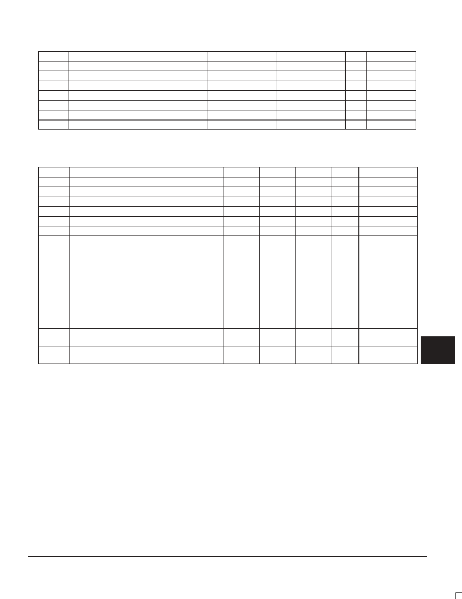
Table 3. Absolute Maximum Ratingsa
Symbol
Characteristics
Min
Max
Unit
Condition
VCC
Supply Voltage
-0.3
3.6
V
VIN
DC Input Voltage
-0.3
VCC + 0.3
V
VOUT
DC Output Voltage
-0.3
VCC + 0.3
V
IIN
DC Input Current
±20
mA
IOUT
DC Output Current
±50
mA
TS
Storage temperature
-65
125
°C
TFunc
Functional temperature range
TA = -40
TJ = +110
°C
a. Absolute maximum continuous ratings are those maximum values beyond which damage to the device may occur. Exposure to these conditions
or conditions beyond those indicated may adversely affect device reliability. Functional operation at absolute-maximum-rated conditions is not
implied.
Table 4. General Specifications
Symbol
Characteristics
Min
Typ
Max
Unit
Condition
VTT
Output termination voltage
VCC – 2a
V
MM
ESD Protection (Machine model)
200
V
HBM
ESD Protection (Human body model)
4000
V
CDM
ESD Protection (Charged device model
2000
V
LU
Latch-up immunity
200
mA
CIN
4.0
pF
Inputs
θJA
Thermal resistance junction to ambient
JESD 51-3, single layer test board
JESD 51-6, 2S2P multilayer test board
83.1
73.3
68.9
63.8
57.4
59.0
54.4
52.5
50.4
47.8
86.0
75.4
70.9
65.3
59.6
60.6
55.7
53.8
51.5
48.8
°C/W
Natural convection
100 ft/min
200 ft/min
400 ft/min
800 ft/min
Natural convection
100 ft/min
200 ft/min
400 ft/min
800 ft/min
θJC
Thermal resistance junction to case
23.0
26.3
°C/W
MIL-SPEC 883E
Method 1012.1
TJ
Operating junction temperatureb (continuous
operation)MTBF = 9.1 years
110
°C
a. Output termination voltage VTT = 0V for VCC = 2.5V operation is supported but the power consumption of the device will increase
b. Operating junction temperature impacts device life time. Maximum continues operating junction temperature should be selected according
to the application life time requirements (See application note AN1545 and the application section in this datasheet for more information).
The device AC and DC parameters are specified up to 110
°C junction temperature allowing the MC100ES6111 to be used in applications
requiring industrial temperature range. It is recommended that users of the MC100ES6111 employ thermal modeling analysis to assist in
applying the junction temperature specifications to their particular application.
相关PDF资料 |
PDF描述 |
|---|---|
| MC100ES6111FA | 100E SERIES, LOW SKEW CLOCK DRIVER, 10 TRUE OUTPUT(S), 0 INVERTED OUTPUT(S), PQFP32 |
| MC100ES6139DWR2 | 100E SERIES, LOW SKEW CLOCK DRIVER, 4 TRUE OUTPUT(S), 0 INVERTED OUTPUT(S), PDSO20 |
| MC100ES6220TBR2 | 100E SERIES, LOW SKEW CLOCK DRIVER, 10 TRUE OUTPUT(S), 0 INVERTED OUTPUT(S), PQFP52 |
| MC100ES6221AER2 | 100E SERIES, LOW SKEW CLOCK DRIVER, 20 TRUE OUTPUT(S), 0 INVERTED OUTPUT(S), PQFP52 |
| MC100ES6221AE | 100E SERIES, LOW SKEW CLOCK DRIVER, 20 TRUE OUTPUT(S), 0 INVERTED OUTPUT(S), PQFP52 |
相关代理商/技术参数 |
参数描述 |
|---|---|
| MC100ES6130DT | 功能描述:时钟驱动器及分配 Buffer RoHS:否 制造商:Micrel 乘法/除法因子:1:4 输出类型:Differential 最大输出频率:4.2 GHz 电源电压-最大: 电源电压-最小:5 V 最大工作温度:+ 85 C 封装 / 箱体:SOIC-8 封装:Reel |
| MC100ES6130EJ | 功能描述:时钟缓冲器 FSL 1-10 Diff LVPECL Fanout Buffer RoHS:否 制造商:Texas Instruments 输出端数量:5 最大输入频率:40 MHz 传播延迟(最大值): 电源电压-最大:3.45 V 电源电压-最小:2.375 V 最大功率耗散: 最大工作温度:+ 85 C 最小工作温度:- 40 C 封装 / 箱体:LLP-24 封装:Reel |
| MC100ES6130EJR2 | 功能描述:时钟缓冲器 FSL 1-10 Diff LVPECL Fanout Buffer RoHS:否 制造商:Texas Instruments 输出端数量:5 最大输入频率:40 MHz 传播延迟(最大值): 电源电压-最大:3.45 V 电源电压-最小:2.375 V 最大功率耗散: 最大工作温度:+ 85 C 最小工作温度:- 40 C 封装 / 箱体:LLP-24 封装:Reel |
| MC100ES6139DT | 功能描述:时钟发生器及支持产品 Buffer RoHS:否 制造商:Silicon Labs 类型:Clock Generators 最大输入频率:14.318 MHz 最大输出频率:166 MHz 输出端数量:16 占空比 - 最大:55 % 工作电源电压:3.3 V 工作电源电流:1 mA 最大工作温度:+ 85 C 安装风格:SMD/SMT 封装 / 箱体:QFN-56 |
| MC100ES6139EJ | 功能描述:时钟发生器及支持产品 FSL 1-4 LVPECL Div. 2/4, Div. 4/5/6 Cloc RoHS:否 制造商:Silicon Labs 类型:Clock Generators 最大输入频率:14.318 MHz 最大输出频率:166 MHz 输出端数量:16 占空比 - 最大:55 % 工作电源电压:3.3 V 工作电源电流:1 mA 最大工作温度:+ 85 C 安装风格:SMD/SMT 封装 / 箱体:QFN-56 |
发布紧急采购,3分钟左右您将得到回复。