参数资料
| 型号: | MC100LVEL40DWG |
| 厂商: | ON Semiconductor |
| 文件页数: | 1/6页 |
| 文件大小: | 0K |
| 描述: | IC DETECT PHASE FREQ ECL 20SOIC |
| 标准包装: | 38 |
| 系列: | 100LVEL |
| 类型: | 相频探测器 |
| PLL: | 无 |
| 输入: | CML,LVDS,NECL,PECL |
| 输出: | ECL |
| 电路数: | 1 |
| 比率 - 输入:输出: | 1:3 |
| 差分 - 输入:输出: | 是/是 |
| 频率 - 最大: | 250MHz |
| 除法器/乘法器: | 无/无 |
| 电源电压: | ±3 V ~ 5.5 V |
| 工作温度: | -40°C ~ 85°C |
| 安装类型: | 表面贴装 |
| 封装/外壳: | 20-SOIC(0.295",7.50mm 宽) |
| 供应商设备封装: | 20-SOIC |
| 包装: | 管件 |
| 其它名称: | MC100LVEL40DWGOS |
Semiconductor Components Industries, LLC, 2006
November, 2006 Rev. 8
1
Publication Order Number:
MC100LVEL40/D
MC100LVEL40
3.3/5VECL Differential
PhaseFrequency Detector
Description
The MC100LVEL40 is a three state phase frequencydetector
intended for phaselocked loop applications which require a minimum
amount of phase and frequency difference at lock. Advanced design
significantly reduces the dead zone of the detector. For proper
operation, the input edge rate of the R and V inputs should be less than
5 ns. The device is designed to work with a 3.3 V power supply.
When the reference (R) and the feedback (FB) inputs are unequal in
frequency and/or phase the differential up (U) and down (D) outputs
will provide pulse streams which when subtracted and integrated
provide an error voltage for control of a VCO.
The VBB pin, an internally generated voltage supply, is available to
this device only. For single-ended input conditions, the unused
differential input is connected to VBB as a switching reference voltage.
VBB may also rebias AC coupled inputs. When used, decouple VBB
and VCC via a 0.01 mF capacitor and limit current sourcing or sinking
to 0.5 mA. When not used, VBB should be left open.
For application information, refer to AND8040/D, “Phase Lock
Loop Operation.”
The 100 Series Contains Temperature Compensation
Features
250 MHz Typical Bandwidth
PECL Mode Operating Range:
VCC = 3.0 V to 5.5 V with VEE = 0 V
NECL Mode Operating Range:
VCC = 0 V with VEE = 3.0 V to 5.5 V
Internal Input Pulldown Resistor
PbFree Packages are Available*
*For additional information on our PbFree strategy and soldering details, please
download the ON Semiconductor Soldering and Mounting Techniques
Reference Manual, SOLDERRM/D.
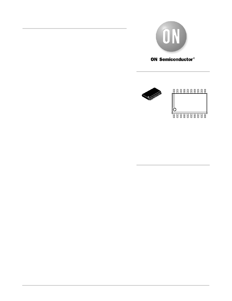
MARKING
DIAGRAM
SO20
DW SUFFIX
CASE 751D
1
20
http://onsemi.com
A
= Assembly Location
WL
= Wafer Lot
YY
= Year
WW
= Work Week
G= PbFree Package
*For additional marking information, refer to
Application Note AND8002/D.
See detailed ordering and shipping information in the package
dimensions section on page 5 of this data sheet.
ORDERING INFORMATION
20
1
100LVEL40
AWLYYWWG
相关PDF资料 |
PDF描述 |
|---|---|
| MC100LVEL56DWR2G | IC MUX 2:1 DUAL DIFF ECL 20-SOIC |
| MC100LVEP05DG | IC GATE AND/NAND ECL 2INP 8SOIC |
| MC100LVEP111MNRG | IC CLK BUFF MUX 2:10 3GHZ 32-QFN |
| MC100LVEP14DT | IC CLOCK BUFFER MUX 2:5 20-TSSOP |
| MC100LVEP210MNG | IC CLOCK BUFFER 1:5 3GHZ 32-QFN |
相关代理商/技术参数 |
参数描述 |
|---|---|
| MC100LVEL40DWR2 | 功能描述:相位探测器 / 移相器 3.3V/5V ECL Diff RoHS:否 制造商:M/A-COM Technology Solutions 封装 / 箱体:PQFN-24 封装:Reel |
| MC100LVEL40DWR2G | 功能描述:相位探测器 / 移相器 3.3V/5V ECL Diff Phase Freq. Detector RoHS:否 制造商:M/A-COM Technology Solutions 封装 / 箱体:PQFN-24 封装:Reel |
| MC100LVEL51D | 功能描述:触发器 3.3V/5V ECL D-Type RoHS:否 制造商:Texas Instruments 电路数量:2 逻辑系列:SN74 逻辑类型:D-Type Flip-Flop 极性:Inverting, Non-Inverting 输入类型:CMOS 输出类型: 传播延迟时间:4.4 ns 高电平输出电流:- 16 mA 低电平输出电流:16 mA 电源电压-最大:5.5 V 最大工作温度:+ 85 C 安装风格:SMD/SMT 封装 / 箱体:X2SON-8 封装:Reel |
| MC100LVEL51DG | 功能描述:触发器 3.3V/5V ECL D-Type w/Diff Clock RoHS:否 制造商:Texas Instruments 电路数量:2 逻辑系列:SN74 逻辑类型:D-Type Flip-Flop 极性:Inverting, Non-Inverting 输入类型:CMOS 输出类型: 传播延迟时间:4.4 ns 高电平输出电流:- 16 mA 低电平输出电流:16 mA 电源电压-最大:5.5 V 最大工作温度:+ 85 C 安装风格:SMD/SMT 封装 / 箱体:X2SON-8 封装:Reel |
| MC100LVEL51DR2 | 功能描述:触发器 3.3V/5V ECL D-Type RoHS:否 制造商:Texas Instruments 电路数量:2 逻辑系列:SN74 逻辑类型:D-Type Flip-Flop 极性:Inverting, Non-Inverting 输入类型:CMOS 输出类型: 传播延迟时间:4.4 ns 高电平输出电流:- 16 mA 低电平输出电流:16 mA 电源电压-最大:5.5 V 最大工作温度:+ 85 C 安装风格:SMD/SMT 封装 / 箱体:X2SON-8 封装:Reel |
发布紧急采购,3分钟左右您将得到回复。