- 您现在的位置:买卖IC网 > PDF目录371008 > MC13110AFB (MOTOROLA INC) UNIVERSAL NARROWBAND FM RECEIVER INTEGRATED CIRCUIT PDF资料下载
参数资料
| 型号: | MC13110AFB |
| 厂商: | MOTOROLA INC |
| 元件分类: | 无绳电话/电话 |
| 英文描述: | UNIVERSAL NARROWBAND FM RECEIVER INTEGRATED CIRCUIT |
| 中文描述: | TELECOM, CORDLESS, RF AND BASEBAND CIRCUIT, PQFP52 |
| 封装: | PLASTIC, QFP-52 |
| 文件页数: | 39/68页 |
| 文件大小: | 1316K |
| 代理商: | MC13110AFB |
第1页第2页第3页第4页第5页第6页第7页第8页第9页第10页第11页第12页第13页第14页第15页第16页第17页第18页第19页第20页第21页第22页第23页第24页第25页第26页第27页第28页第29页第30页第31页第32页第33页第34页第35页第36页第37页第38页当前第39页第40页第41页第42页第43页第44页第45页第46页第47页第48页第49页第50页第51页第52页第53页第54页第55页第56页第57页第58页第59页第60页第61页第62页第63页第64页第65页第66页第67页第68页
MC13110A/B MC13111A/B
PLL SYNTHESIZER SECTION
39
MOTOROLA ANALOG IC DEVICE DATA
PLL Frequency Synthesizer General Description
Figure 95 shows a simplified block diagram of the
programmable universal dual phase locked loop (PLL)
designed into the MC13110A/B and MC13111A/B IC. This
dual PLL is fully programmable through the MCU serial
interface and supports most country channel frequencies
including USA (25 ch), Spain, Australia, Korea, New Zealand,
U.K., Netherlands, France, and China (see channel frequency
tables in AN1575, “Worldwide Cordless Telephone
Frequencies”).
The 2nd local oscillator and reference divider provide the
reference frequency signal for the Rx and Tx PLL loops. The
programmed divider value for the reference divider is
selected based on the crystal frequency and the desired Rx
and Tx reference frequency values. For the U.K., additional
divide by 25 and divide by 4 blocks are provided to allow for
generation of the 1.0 kHz and 6.2 kHz reference frequencies.
The 14–bit Rx counter is programmed for the desired first
local oscillator frequency. The 14–bit Tx counter is
programmed for the desired transmit channel frequency. All
counters power–up to a set default state for USA channel #21
using a 10.24 MHz reference frequency crystal (see power–up
default latch register state in the Serial Programmable
Interface section).
To extend the sensitivity of the 1st LO for U.S. 25 channel
operation, internal fixed capacitors can be connected to the
tank circuit through microprocessor programmable control.
When designing the external PLL loop filters, it is
recommended that the Tx and Rx phase detectors be
considered as current drive type outputs. The loop filter
control voltage must be 0.5 V away from either the positive or
negative supply rail.
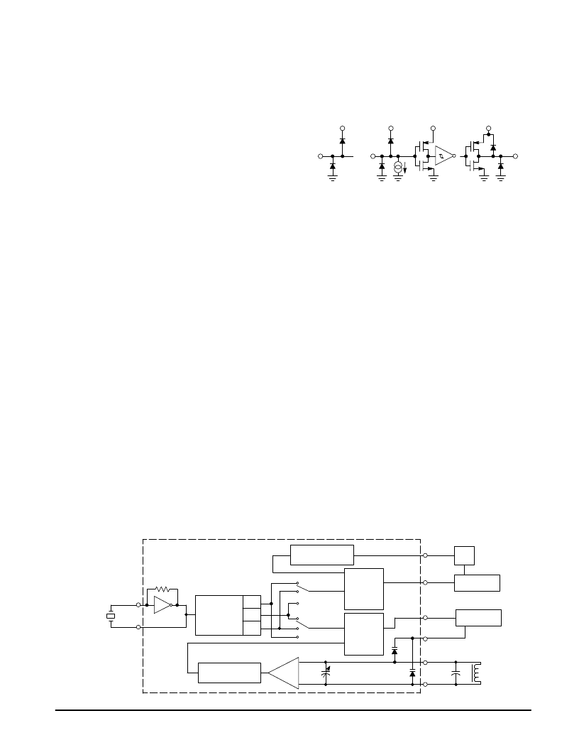
PLL I/O Pin Configurations
The 2nd LO, Rx and Tx PLL’s, and MPU serial interface are
powered by the internal voltage regulator at the “PLL Vref” pin.
The “PLL Vref” pin is the output of a voltage regulator which is
powered from the “VCC Audio” power supply pin. It is regulated
by an internal bandgap voltage reference. Therefore, the
maximum input and output levels for most of the PLL I/O pins
(LO2 In, LO2 Out, Rx PD, Tx PD, Tx VCO) is the regulated
voltage at the “PLL Vref” pin. The ESD protection diodes on
these pins are also connected to “PLL Vref”.
Internal level shift buffers are provided for the pins (Data,
Clk, EN, Clk Out) which connect directly to the
microprocessor. The maximum input and output levels for
these pins is VCC. Figure 94 shows a simplified schematic of
the I/O pins.
Figure 94. PLL I/O Pin Simplified Schematics
PLL Vref
(2.5 V)
In
I/O
VCC Audio
(2.7 to 5.5 V)
PLL Vref
(2.5 V)
VCC Audio
(2.7 to 5.5 V)
Clk Out Pin
Data, Clk and EN Pins
LO2 In, LO2 Out,
Rx PD, Tx PD and
Tx VCO Pins
Out
2.0
μ
A
PLL Loop Control Voltage Range
The control voltage for the Tx and Rx loop filters is set by
the phase detector outputs which drive the external loop
filters. The phase detectors are best considered to have a
current mode type output. The output can have three states;
ground, high impedance, and positive supply, which in this
case is the voltage at “PLL Vref”. When the loop is locked the
phase detector outputs are at high impedance. An exception
of this state is for narrow current pulses, referenced to either
the positive or negative supply rails. If the loop voltages get
within 0.5 V of either rail the linear current output starts to
degrade. The phase detector current source was not
designed to operate at the supply rails. VCO tuning range will
also be limited by this voltage range
The maximum loop control voltage is the “PLL Vref” voltage
which is 2.5 V. If a higher loop control voltage range is
desired, the “PLL Vref” pin can be pulled to a higher voltage.
It can be tied directly to the VCC voltage (with suitable filter
capacitors connected close to each pin). When this is done,
the internal voltage regulator is automatically disabled. This
is commonly used in the telephone base set where an
external 5.0 V regulated voltage is available. It is important to
remember, that if “PLL Vref” is tied to VCC and VCC is not a
regulated voltage, the PLL loop parameters and lock–up time
will vary with supply voltage variation. The phase detector
gain constant, Kpd, will not be affected if the “PLL Vref” is tied
to VCC.
Figure 95. Dual PLL Simplified Block Diagram
14–b Programmable
Rx Counter
14–b Programmable
Tx Counter
12–b
Programmable
Reference
Counter
÷
25
÷
4
÷
1
LO2 In
LO2 Out
1
2
Tx PD
8
6
Tx VCO
Rx PD
4
Vcap Ctrl
42
LO1 In
40
LO1 Out
41
Tx Phase
Detector
(Current
Output)
Rx Phase
Detector
(Current
Output)
LP Loop Filter
Tx Ref
Rx Ref
U.K. Base
U.K. Handset
U.K. Base
U.K. Handset
1st LO
LP Loop Filter
Tx
VCO
Programmable
Internal Capacitor
相关PDF资料 |
PDF描述 |
|---|---|
| MC13110AFTA | UNIVERSAL NARROWBAND FM RECEIVER INTEGRATED CIRCUIT |
| MC13110BFB | UNIVERSAL NARROWBAND FM RECEIVER INTEGRATED CIRCUIT |
| MC13111AFB | UNIVERSAL NARROWBAND FM RECEIVER INTEGRATED CIRCUIT |
| MC13110BFTA | UNIVERSAL NARROWBAND FM RECEIVER INTEGRATED CIRCUIT |
| MC13111AFTA | UNIVERSAL NARROWBAND FM RECEIVER INTEGRATED CIRCUIT |
相关代理商/技术参数 |
参数描述 |
|---|---|
| MC13110AFTA | 制造商:MOTOROLA 制造商全称:Motorola, Inc 功能描述:UNIVERSAL NARROWBAND FM RECEIVER INTEGRATED CIRCUIT |
| MC13110BFB | 制造商:MOTOROLA 制造商全称:Motorola, Inc 功能描述:UNIVERSAL NARROWBAND FM RECEIVER INTEGRATED CIRCUIT |
| MC13110BFTA | 制造商:Motorola 功能描述:MOTOROLA 9942 |
| MC13111AFB | 制造商:MOTOROLA 制造商全称:Motorola, Inc 功能描述:UNIVERSAL NARROWBAND FM RECEIVER INTEGRATED CIRCUIT |
| MC13111AFTA | 制造商:MOTOROLA 制造商全称:Motorola, Inc 功能描述:UNIVERSAL CORDLESS TELEPHONE SUBSYSTEM IC |
发布紧急采购,3分钟左右您将得到回复。