- 您现在的位置:买卖IC网 > PDF目录2012 > MC144111DWR2 (Freescale Semiconductor)IC QUAD SERIAL D/A CONV 16-SOIC PDF资料下载
参数资料
| 型号: | MC144111DWR2 |
| 厂商: | Freescale Semiconductor |
| 文件页数: | 7/12页 |
| 文件大小: | 0K |
| 描述: | IC QUAD SERIAL D/A CONV 16-SOIC |
| 标准包装: | 1,000 |
| 位数: | 6 |
| 数据接口: | 串行 |
| 转换器数目: | 4 |
| 电压电源: | 双 ± |
| 功率耗散(最大): | 50mW |
| 工作温度: | 0°C ~ 85°C |
| 安装类型: | 表面贴装 |
| 封装/外壳: | 16-SOIC(0.295",7.50mm 宽) |
| 供应商设备封装: | 16-SOIC W |
| 包装: | 带卷 (TR) |
| 输出数目和类型: | 8 电压,单极 |
| 采样率(每秒): | * |
| 其它名称: | MC144111DWTR |
MC144110 Technical Data, Rev. 2
4
Freescale Semiconductor
Electrical Specifications
2
Electrical Specifications
This device contains protection circuitry to guard against damage due to high static voltages or electric
fields; however, it is advised that precautions be taken to avoid application of voltage higher than
maximum rated voltages to this high-impedance circuit. For proper operation it is recommended that Vin
and Vout be constrained to the range VSS ≤ (Vin or Vout) ≤VDD.
Unused inputs must always be tied to an appropriate logic voltage level (e.g., either VSS or VDD).
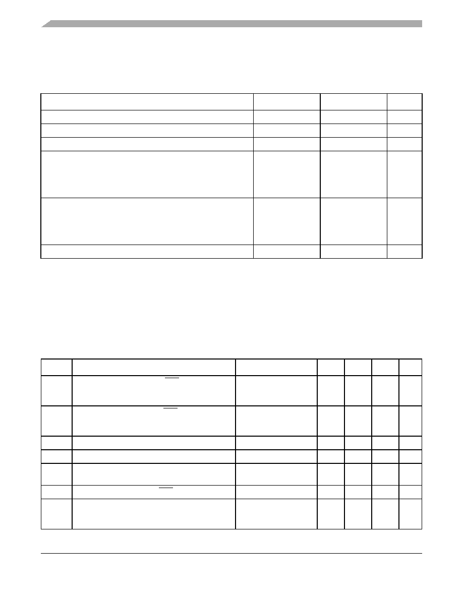
Table 1. Maximum Ratings
(Voltages referenced to VSS)
Ratings
Symbol
Value
Unit
DC Supply Voltage
VDD
- 0.5 to + 18
V
Input Voltage, All Inputs
Vin
- 0.5 to VDD + 0.5
V
DC Input Current, per Pin
I
± 10
mA
Power Dissipation (Per Output)
TA = 70°C
MC144110
MC144111
TA = 85°C
MC144110
MC144111
POH
30
50
10
20
mW
Power Dissipation (Per Package)
TA = 70°C
MC144110
MC144111
TA = 85°C
MC144110
MC144111
PD
100
150
25
50
mW
Storage Temperature Range
Tstg
- 65 to + 150
°C
Table 2. Electrical Characteristics
(Voltages referenced to VSS, TA = 0 to 85°C unless otherwise indicated)
Symbol
Parameter
Test Conditions
VDD
Min
Max
Unit
VIH
High-Level Input Voltage (Din, ENB, CLK)
5
10
15
3.0
3.5
4
-
V
VIL
Low-Level Input Voltage (Din, ENB, CLK)
5
10
15
-
0.8
V
IOH
High-Level Output Current (Dout)
Vout = VDD - 0.5 V
5
- 200
-
A
IOL
Low-Level Output Current (Dout)
Vout = 0.5 V
5
200
-
A
IDD
Quiescent Supply Current
MC144110
MC144111
Iout = 0 A
15
-
12
8
mA
Iin
Input Leakage Current (Din, ENB, CLK)
Vin = VDD or 0 V
15
-
± 1
A
Vnonl
Nonlinearity Voltage (Rn Out)
See Figure 3
5
10
15
-
100
200
300
mV
相关PDF资料 |
PDF描述 |
|---|---|
| MC145152DW2R2 | IC PAR-IN PLL FREQ SYNTH 28-SOIC |
| MC14536BFEL | IC OSC PROG TIMER 2MHZ 16SOEIAJ |
| MC14541BFG | IC OSC PROG TIMER 3MHZ 14SOEIAJ |
| MC145423EJ | IC TXRX UDLT/ISDN 28-TSSOP |
| MC145481ENR2 | IC CODEC-FILTER PCM 3V 20-SSOP |
相关代理商/技术参数 |
参数描述 |
|---|---|
| MC144111P | 制造商:Motorola Inc 功能描述: |
| MC14411L | 制造商: 功能描述: 制造商:undefined 功能描述: |
| MC14411P | 制造商:Motorola 功能描述:MOTOROLA |
| MC14412FP | 制造商:Motorola Inc 功能描述: |
| MC14413P2 | 制造商:Motorola Inc 功能描述: |
发布紧急采购,3分钟左右您将得到回复。