- 您现在的位置:买卖IC网 > PDF目录371012 > MC144112D (MOTOROLA INC) Quad Six-Bit Digital-to-Analog Converter PDF资料下载
参数资料
| 型号: | MC144112D |
| 厂商: | MOTOROLA INC |
| 元件分类: | DAC |
| 英文描述: | Quad Six-Bit Digital-to-Analog Converter |
| 中文描述: | QUAD, SERIAL INPUT LOADING, 6-BIT DAC, PDSO14 |
| 封装: | SOG-14 |
| 文件页数: | 2/6页 |
| 文件大小: | 83K |
| 代理商: | MC144112D |
MC144112
2
MOTOROLA
áááááááááááááááááááá
áááááááááááááááááááá
á
ááááááááááá
á
á
ááááááááááá
áááááááááááááááááááá
á
á
áááááááááááááááááááá
áá
áá
áá
áááááááááááááááááááá
ááááá
50
20
áááááááááááááááááááá
ááááááááá
TA = 70
°
C
TA = 85
C
á
á
ááááá
ááááá
50
– 65 to + 150
á
á
°
C
á
á
ááááááááá
ááááááááá
TA = 85
°
C
á
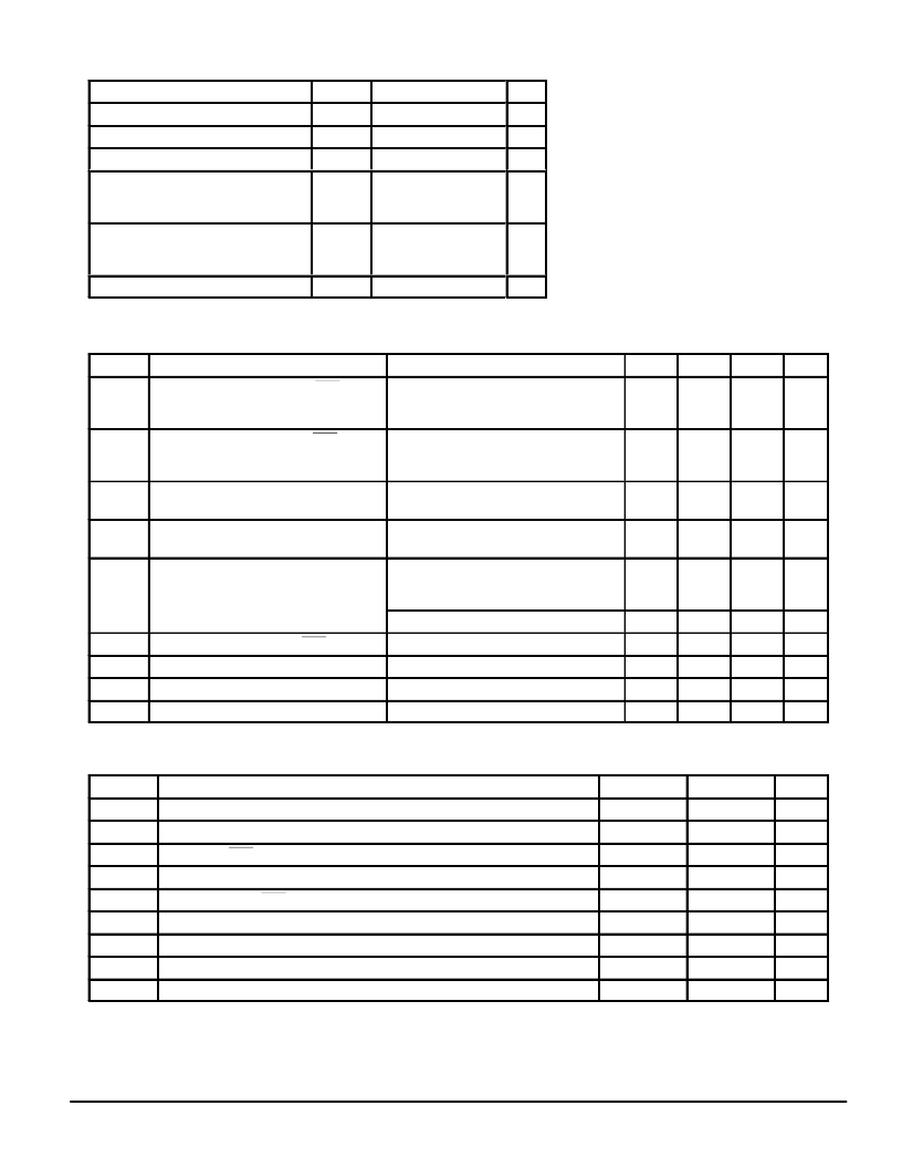
Power Dissipation (Per Package)
°
á
PD
á
á
á
á
mW
Storage Temperature Range
ELECTRICAL CHARACTERISTICS
(Voltages referenced to VSS, VDD = 2.7 to 5.5 V, TA = – 40 to 85
°
C unless otherwise indicated)
Symbol
Parameter
Test Conditions
VDD
2.7
4.5
5.5
Min
Max
Unit
VIH
High–Level Input Voltage (Din, ENB, CLK)
2.03
3.15
3.85
—
—
—
V
VIL
Low–Level Input Voltage (Din, ENB, CLK)
2.7
4.5
5.5
—
—
—
0.67
1.35
1.65
V
IOH
High–Level Output Current (Dout)
Vout = VDD – 0.5 V
2.7
4.5
0.3
1.1
—
—
mA
IOL
Low–Level Output Current (Dout)
Vout = 0.5 V
2.7
4.5
1.0
1.8
—
—
mA
ISS
Quiescent Supply Current (per Package)
Iout = 0
μ
A, All DAC Outputs = Zero
2.7
4.5
5.5
—
—
—
1.25
2.10
2.50
mA
Iout = 0
μ
A, All DAC Outputs = Full Scale
5.5
—
30
μ
A
Iin
Input Leakage Current (Din, ENB, CLK)
Integral Nonlinearity (Rn Out)
Vin = VDD or 0 V
See Figure 1
5.5
—
1
μ
A
Vnonl
Vstep
Voffset
—
– 1
1/4
1/4
LSB
Differential Nonlinearity (Rn Out)
See Figure 2
—
–
3/4
3/4
LSB
Offset from VSS
Din = $00, See Figure 1
—
1/4
1
3/4
LSB
SWITCHING CHARACTERISTICS
(VDD = 2.7 to 5.5 V, Voltages referenced to VSS, TA = – 40 to 85
°
C, CL = 50 pF, Input tr = tf = 20 ns unless otherwise indicated)
Symbol
Parameter
Min
Max
Unit
twH
twL
tsu
tsu
th
th
tr, tf
Cin
fclk
Positive Pulse Width, CLK (Figures 3 and 4)
166
—
ns
Negative Pulse Width, CLK (Figures 3 and 4)
166
—
ns
Setup Time, ENB to CLK (Figures 3 and 4)
135
—
ns
Setup Time, Din to CLK (Figures 3 and 4)
Hold Time, CLK to ENB (Figures 3 and 4)
55
—
ns
135
—
ns
Hold Time, CLK to Din (Figures 3 and 4)
Input Rise and Fall Times, CLK
55
—
ns
—
100
μ
s
Input Capacitance
—
10
pF
Serial Data Clock Frequency (Refer to twH and twL Above) (Figures 3 and 4)
dc
3
MHz
This device contains protection circuitry to
guard against damage due to high static
voltages or electric fields; however, it is ad-
vised that precautions be taken to avoid
application of voltage higher than maximum
rated voltages to this high–impedance circuit.
For proper operation it is recommended that
Vin and Vout be constrained to the range VSS
≤
(Vin or Vout)
≤
VDD.
Unused inputs must always be tied to an
appropriate logic voltage level (e.g., either VSS
or VDD).
相关PDF资料 |
PDF描述 |
|---|---|
| MC144112 | 30 AMP MINIATURE POWER RELAY |
| MC14411L | Enhanced Product Fixed-Point Digital Signal Processor 532-FCBGA -40 to 105 |
| MC14411P | CMOS LSI |
| MC14412FL | UNIVERSAL LOW SPEED MODEM(0-600 bps) |
| MC14412FP | SM34020APCM40 144-QFP |
相关代理商/技术参数 |
参数描述 |
|---|---|
| MC14411L | 制造商: 功能描述: 制造商:undefined 功能描述: |
| MC14411P | 制造商:Motorola 功能描述:MOTOROLA |
| MC14412FP | 制造商:Motorola Inc 功能描述: |
| MC14413P2 | 制造商:Motorola Inc 功能描述: |
| MC144143P1 | 制造商:Panasonic Industrial Company 功能描述:IC |
发布紧急采购,3分钟左右您将得到回复。