- 您现在的位置:买卖IC网 > PDF目录371012 > MC144112D (MOTOROLA INC) Quad Six-Bit Digital-to-Analog Converter PDF资料下载
参数资料
| 型号: | MC144112D |
| 厂商: | MOTOROLA INC |
| 元件分类: | DAC |
| 英文描述: | Quad Six-Bit Digital-to-Analog Converter |
| 中文描述: | QUAD, SERIAL INPUT LOADING, 6-BIT DAC, PDSO14 |
| 封装: | SOG-14 |
| 文件页数: | 5/6页 |
| 文件大小: | 83K |
| 代理商: | MC144112D |
MC144112
MOTOROLA
5
PIN DESCRIPTIONS
INPUTS
Din
Data Input
Four 6–bit words are entered serially, MSB first, into the
digital data input, Din.
The last 6–bit word shifted in determines the output level of
pin R1 Out. The next–to–last 6–bit word affects pin R2 Out,
etc.
ENB
Negative Logic Enable
The ENB pin must be low (active) during the serial load.
On the low–to–high transition of ENB, data contained in the
shift register is loaded into the latch.
CLK
Shift Register Clock
Data is shifted into the register on the high–to–low transi-
tion of CLK. CLK is fed into the D–input of a transparent
latch, which is used for inhibiting the clocking of the shift reg-
ister when ENB is high.
The MC144112 usually uses 24 CLK cycles. See Table 1
for additional information.
OUTPUTS
Dout
Data Output
The digital data output is primarily used for cascading the
DACs and may be fed into Din of the next stage.
If not used, the output should be floated.
R1 Out through R4 Out
Resistor Network Outputs
These are the R–2R resistor network outputs. These out-
puts may be fed to high–impedance loads. The R value of
the resistor network ranges from 7 to 15 k
.
If not used, an output should be floated.
SUPPLY PINS
VSS
Negative Supply Voltage
This pin is usually ground.
VDD
Positive Supply Voltage
The voltage applied to this pin determines the analog out-
put swing. The DAC output voltage range is from approxi-
mately VSS to VDD.
APPLICATIONS INFORMATION
For those applications where supply current is critical, any
unused DAC channels should be programmed for full–scale
output. The unused outputs are floated (no connects).
For example, with a 4.5 V supply, the worst case current
when all DACs are programmed for zero output is 2.1 mA.
This is 2.1 mA for the package; each DAC is drawing 1/4 of
this, or 525
μ
A. If only two channels are needed, minimum
supply current is achieved by programming the two unused
channels to full–scale output (all ones). In this case, the
worst case supply current is approximately two times
525
μ
A, or 1.05 mA.
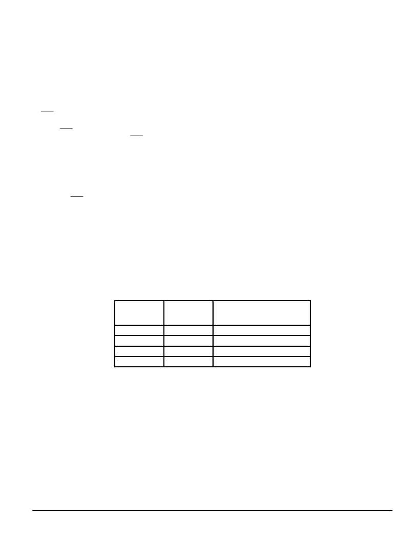
Table 1. Number of Channels vs Clocks Required
Number of
Channels
Required
Minimum
Number of
Clock Cycles*
Outputs Used
1
6
R1 Out
2
12
R1 Out, R2 Out
3
18
R1 Out, R2 Out, R3 Out
4
24
R1 Out, R2 Out, R3 Out, R4 Out
* Additional clock cycles can be used, with the leading extra bits being don’t cares.
For example, eight clocks can be used if one channel is needed. The first two bits
are don’t cares; the last six bits determine the DAC output.
相关PDF资料 |
PDF描述 |
|---|---|
| MC144112 | 30 AMP MINIATURE POWER RELAY |
| MC14411L | Enhanced Product Fixed-Point Digital Signal Processor 532-FCBGA -40 to 105 |
| MC14411P | CMOS LSI |
| MC14412FL | UNIVERSAL LOW SPEED MODEM(0-600 bps) |
| MC14412FP | SM34020APCM40 144-QFP |
相关代理商/技术参数 |
参数描述 |
|---|---|
| MC14411L | 制造商: 功能描述: 制造商:undefined 功能描述: |
| MC14411P | 制造商:Motorola 功能描述:MOTOROLA |
| MC14412FP | 制造商:Motorola Inc 功能描述: |
| MC14413P2 | 制造商:Motorola Inc 功能描述: |
| MC144143P1 | 制造商:Panasonic Industrial Company 功能描述:IC |
发布紧急采购,3分钟左右您将得到回复。