参数资料
| 型号: | MC14536BDWR2G |
| 厂商: | ON Semiconductor |
| 文件页数: | 10/14页 |
| 文件大小: | 0K |
| 描述: | IC OSC PROG TIMER 2MHZ 16SOIC |
| 标准包装: | 1 |
| 类型: | 可编程计时器 |
| 频率: | 2MHz |
| 电源电压: | 3 V ~ 18 V |
| 电流 - 电源: | 15µA |
| 工作温度: | -55°C ~ 125°C |
| 封装/外壳: | 16-SOIC(0.295",7.50mm 宽) |
| 包装: | 标准包装 |
| 供应商设备封装: | 16-SOIC W |
| 安装类型: | 表面贴装 |
| 产品目录页面: | 1125 (CN2011-ZH PDF) |
| 其它名称: | MC14536BDWR2GOSDKR |
MC14536B
http://onsemi.com
5
PIN DESCRIPTIONS
INPUTS
SET (Pin 1) A high on Set asynchronously forces Decode
Out to a high level. This is accomplished by setting an output
conditioning latch to a high level while at the same time
resetting the 24 flipflop stages. After Set goes low (inactive),
the occurrence of the first negative clock transition on IN1
causes Decode Out to go low. The counter’s flipflop stages
begin counting on the second negative clock transition of IN1.
When Set is high, the onchip RC oscillator is disabled. This
allows for very lowpower standby operation.
RESET (Pin 2) A high on Reset asynchronously forces
Decode Out to a low level; all 24 flipflop stages are also reset
to a low level. Like the Set input, Reset disables the onchip
RC oscillator for standby operation.
IN1 (Pin 3) The device’s internal counters advance on the
negativegoing edge of this input. IN1 may be used as an
external clock input or used in conjunction with OUT1 and
OUT2 to form an RC oscillator. When an external clock is
used, both OUT1 and OUT2 may be left unconnected or used
to drive 1 LSTTL or several CMOS loads.
8BYPASS (Pin 6) A high on this input causes the first 8
flipflop stages to be bypassed. This device essentially
becomes a 16stage counter with all 16 stages selectable.
Selection is accomplished by the A, B, C, and D inputs. (See
the truth tables.)
CLOCK INHIBIT (Pin 7) A high on this input
disconnects the first counter stage from the clocking source.
This holds the present count and inhibits further counting.
However, the clocking source may continue to run.
Therefore, when Clock Inhibit is brought low, no oscillator
startup time is required. When Clock Inhibit is low, the
counter will start counting on the occurrence of the first
negative edge of the clocking source at IN1.
OSC INHIBIT (Pin 14) A high level on this pin stops the
RC oscillator which allows for very lowpower standby
operation. May also be used, in conjunction with an external
clock, with essentially the same results as the Clock Inhibit
input.
MONOIN (Pin 15) Used as the timing pin for the
onchip monostable multivibrator. If the MonoIn input is
connected to VSS, the monostable circuit is disabled, and
Decode Out is directly connected to the selected Q output.
The monostable circuit is enabled if a resistor is connected
between MonoIn and VDD. This resistor and the device’s
internal capacitance will determine the minimum output
pulse widths. With the addition of an external capacitor to
VSS, the pulse width range may be extended. For reliable
operation the resistor value should be limited to the range of
5 k
W to 100 kW and the capacitor value should be limited to
A, B, C, D (Pins 9, 10, 11, 12) These inputs select the
flipflop stage to be connected to Decode Out. (See the truth
tables.)
OUTPUTS
OUT1, OUT2 (Pin 4, 5) Outputs used in conjunction with
IN1 to form an RC oscillator. These outputs are buffered and
may be used for 20 frequency division of an external clock.
DECODE OUT (Pin 13) Output function depends on
configuration. When the monostable circuit is disabled, this
output is a 50% duty cycle square wave during free run.
TEST MODE
The test mode configuration divides the 24 flipflop
stages into three 8stage sections to facilitate a fast test
sequence. The test mode is enabled when 8Bypass, Set and
Reset are at a high level. (See Figure 10.)
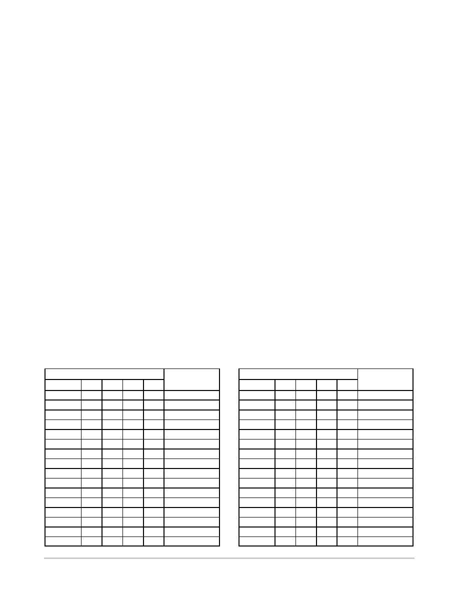
TRUTH TABLES
Input
Stage Selected
for Decode Out
8Bypass
D
C
B
A
0
9
0
1
10
0
1
0
11
0
1
12
0
1
0
13
0
1
0
1
14
0
1
0
15
0
1
16
0
1
0
17
0
1
0
1
18
0
1
0
1
0
19
0
1
0
1
20
0
1
0
21
0
1
0
1
22
0
1
0
23
0
1
24
Input
Stage Selected
for Decode Out
8Bypass
D
C
B
A
1
0
1
0
1
2
1
0
1
0
3
1
0
1
4
1
0
1
0
5
1
0
1
0
1
6
1
0
1
0
7
1
0
1
8
1
0
9
1
0
1
10
1
0
1
0
11
1
0
1
12
1
0
13
1
0
1
14
1
0
15
1
16
相关PDF资料 |
PDF描述 |
|---|---|
| VE-B6F-IU | CONVERTER MOD DC/DC 72V 200W |
| PI3B16233AEX | IC 16:32-BIT FET BUS SW 56-TSSOP |
| VE-B6D-IU | CONVERTER MOD DC/DC 85V 200W |
| VE-B64-IU | CONVERTER MOD DC/DC 48V 200W |
| PI3C3126QE | IC 4-BIT BUS SW 2-PORT 16-QSOP |
相关代理商/技术参数 |
参数描述 |
|---|---|
| MC14536BFEL | 功能描述:计时器和支持产品 LOG CMOS OSILATR TIMER RoHS:否 制造商:Micrel 类型:Standard 封装 / 箱体:SOT-23 内部定时器数量:1 电源电压-最大:18 V 电源电压-最小:2.7 V 最大功率耗散: 最大工作温度:+ 85 C 最小工作温度:- 40 C 封装:Reel |
| MC14536BFELG | 功能描述:计时器和支持产品 LOG CMOS OSILATR TIMER RoHS:否 制造商:Micrel 类型:Standard 封装 / 箱体:SOT-23 内部定时器数量:1 电源电压-最大:18 V 电源电压-最小:2.7 V 最大功率耗散: 最大工作温度:+ 85 C 最小工作温度:- 40 C 封装:Reel |
| MC14538B | 制造商: 功能描述: 制造商:undefined 功能描述: |
| MC14538BBEBS | 制造商: 功能描述: 制造商:undefined 功能描述: |
| MC14538BCP | 功能描述:单稳态多谐振荡器 3-18V Dual Precision RoHS:否 制造商:Texas Instruments 每芯片元件:1 逻辑系列:LVC 逻辑类型:Monostable Multivibrator 封装 / 箱体:SSOP-8 传播延迟时间:18.6 ns 高电平输出电流:- 32 mA 低电平输出电流:32 mA 电源电压-最大:5.5 V 电源电压-最小:1.65 V 最大功率耗散: 最大工作温度:+ 85 C 最小工作温度:- 40 C 封装:Reel |
发布紧急采购,3分钟左右您将得到回复。