参数资料
| 型号: | MC14538BFG |
| 厂商: | ON Semiconductor |
| 文件页数: | 9/14页 |
| 文件大小: | 0K |
| 描述: | IC MULTIVIBRATOR DUAL 16SOEIAJ |
| 标准包装: | 50 |
| 系列: | 4000B |
| 逻辑类型: | 单稳态 |
| 独立电路: | 2 |
| 施密特触发器输入: | 无 |
| 传输延迟: | 95ns |
| 输出电流高,低: | 8.8mA,8.8mA |
| 电源电压: | 3 V ~ 18 V |
| 工作温度: | -55°C ~ 125°C |
| 安装类型: | 表面贴装 |
| 封装/外壳: | 16-SOIC(0.209",5.30mm 宽) |
| 供应商设备封装: | 16-SOEIAJ |
| 包装: | 管件 |
| 其它名称: | MC14538BFG-ND MC14538BFGOS |
MC14538B
http://onsemi.com
4
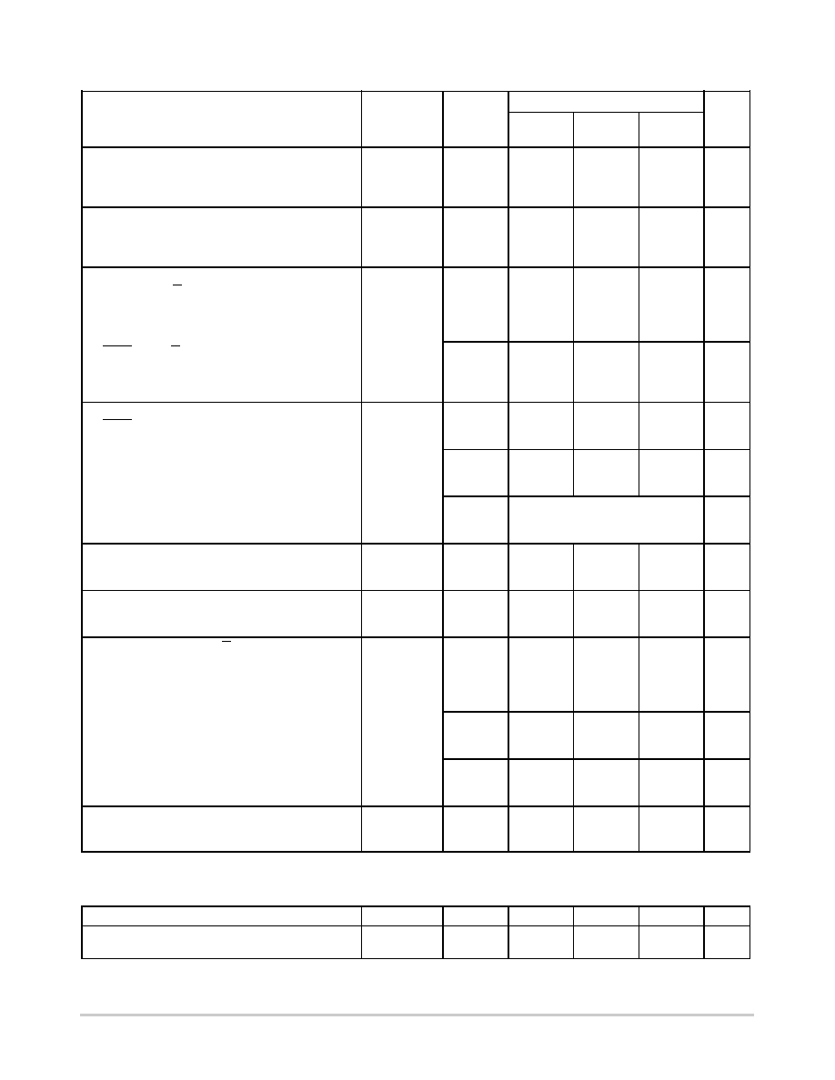
Characteristic
Symbol
VDD
Vdc
All Types
Unit
Min
Typ
(Note 5)
Max
Output Rise Time
tTLH = (1.35 ns/pF) CL + 33 ns
tTLH = (0.60 ns/pF) CL + 20 ns
tTLH = (0.40 ns/pF) CL + 20 ns
tTLH
5.0
10
15
100
50
40
200
100
80
ns
Output Fall Time
tTHL = (1.35 ns/pF) CL + 33 ns
tTHL = (0.60 ns/pF) CL + 20 ns
tTHL = (0.40 ns/pF) CL + 20 ns
tTHL
5.0
10
15
100
50
40
200
100
80
ns
Propagation Delay Time
A or B to Q or Q
tPLH, tPHL = (0.90 ns/pF) CL + 255 ns
tPLH, tPHL = (0.36 ns/pF) CL + 132 ns
tPLH, tPHL = (0.26 ns/pF) CL + 87 ns
tPLH,
tPHL
5.0
10
15
300
150
100
600
300
220
ns
Reset to Q or Q
tPLH, tPHL = (0.90 ns/pF) CL + 205 ns
tPLH, tPHL = (0.36 ns/pF) CL + 107 ns
tPLH, tPHL = (0.26 ns/pF) CL + 82 ns
5.0
10
15
250
125
95
500
250
190
ns
Input Rise and Fall Times
Reset
tr, tf
5
10
15
15
5
4
ms
B Input
5
10
15
300
1.2
0.4
1.0
0.1
0.05
ms
A Input
5
10
15
No Limit
Input Pulse Width
A, B, or Reset
tWH,
tWL
5.0
10
15
170
90
80
85
45
40
ns
Retrigger Time
trr
5.0
10
15
0
ns
Output Pulse Width — Q or Q
Refer to Figures 8 and 9
CX = 0.002 mF, RX = 100 kW
T
5.0
10
15
198
200
202
210
212
214
230
232
234
ms
CX = 0.1 mF, RX = 100 kW
5.0
10
15
9.3
9.4
9.5
9.86
10
10.14
10.5
10.6
10.7
ms
CX = 10 mF, RX = 100 kW
5.0
10
15
0.91
0.92
0.93
0.965
0.98
0.99
1.03
1.04
1.06
s
Pulse Width Match between circuits in
the same package.
CX = 0.1 mF, RX = 100 kW
100
[(T1 – T2)/T1]
5.0
10
15
± 1.0
± 5.0
%
4. The formulas given are for the typical characteristics only at 25_C.
5. Data labelled “Typ” is not to be used for design purposes but is intended as an indication of the IC’s potential performance.
OPERATING CONDITIONS
External Timing Resistance
RX
5.0
(Note 6)
kW
External Timing Capacitance
CX
0
No Limit
(Note 7)
mF
6. The maximum usable resistance RX is a function of the leakage of the capacitor CX, leakage of the MC14538B, and leakage due to board
layout and surface resistance. Susceptibility to externally induced noise signals may occur for RX > 1 MW..
7. If CX > 15 mF, use discharge protection diode per Fig. 11.
相关PDF资料 |
PDF描述 |
|---|---|
| VI-B44-MV-F4 | CONVERTER MOD DC/DC 48V 150W |
| VI-B43-MV-F2 | CONVERTER MOD DC/DC 24V 150W |
| VI-B42-MV-F4 | CONVERTER MOD DC/DC 15V 150W |
| D38999/26WJ19SCLC | CONN HSG PLUG 19POS STRGHT SCKT |
| 74VHC123AM | IC MULTIVIBRATOR MONO DL 16-SOIC |
相关代理商/技术参数 |
参数描述 |
|---|---|
| MC14538BFL1 | 制造商:Rochester Electronics LLC 功能描述:- Bulk |
| MC14538BFL2 | 制造商:Rochester Electronics LLC 功能描述:- Bulk |
| MC14538BFR1 | 制造商:Rochester Electronics LLC 功能描述:- Bulk |
| MC14538BFR2 | 制造商:Rochester Electronics LLC 功能描述:- Bulk |
| MC14539BCP | 制造商:Motorola Inc 功能描述: 制造商:Motorola Inc 功能描述:LOGIC MUX, DUAL, 4-INPUT, CMOS, 16 Pin, Plastic, DIP |
发布紧急采购,3分钟左右您将得到回复。