- 您现在的位置:买卖IC网 > PDF目录132987 > MC16V1CPU20B1 (FREESCALE SEMICONDUCTOR INC) 16-BIT, MROM, 20.97 MHz, MICROCONTROLLER, PQFP100 PDF资料下载
参数资料
| 型号: | MC16V1CPU20B1 |
| 厂商: | FREESCALE SEMICONDUCTOR INC |
| 元件分类: | 微控制器/微处理器 |
| 英文描述: | 16-BIT, MROM, 20.97 MHz, MICROCONTROLLER, PQFP100 |
| 封装: | TQFP-100 |
| 文件页数: | 2/128页 |
| 文件大小: | 571K |
| 代理商: | MC16V1CPU20B1 |
第1页当前第2页第3页第4页第5页第6页第7页第8页第9页第10页第11页第12页第13页第14页第15页第16页第17页第18页第19页第20页第21页第22页第23页第24页第25页第26页第27页第28页第29页第30页第31页第32页第33页第34页第35页第36页第37页第38页第39页第40页第41页第42页第43页第44页第45页第46页第47页第48页第49页第50页第51页第52页第53页第54页第55页第56页第57页第58页第59页第60页第61页第62页第63页第64页第65页第66页第67页第68页第69页第70页第71页第72页第73页第74页第75页第76页第77页第78页第79页第80页第81页第82页第83页第84页第85页第86页第87页第88页第89页第90页第91页第92页第93页第94页第95页第96页第97页第98页第99页第100页第101页第102页第103页第104页第105页第106页第107页第108页第109页第110页第111页第112页第113页第114页第115页第116页第117页第118页第119页第120页第121页第122页第123页第124页第125页第126页第127页第128页
MOTOROLA
MC68HC16V1
10
MC68HC16V1TS/D
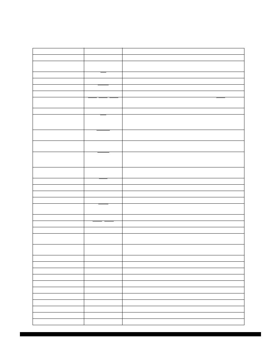
2.5 MC68HC16V1 Signal Function
Table 6 MCU Signal Function
Signal Name
Mnemonic
Function
Address Bus
ADDR[17:0]
18-bit address used by CPU16
Address Latch Enable
ALE
Enables external address latching by indicating when address is
valid on address/data bus
Address Strobe
AS
Indicates that a valid address is on the address bus
Bus Error
BERR
Signals to the SLIM that a bus error has occurred
Breakpoint
BKPT
Signals a hardware breakpoint to the CPU
Clock Out
CLKOUT
System clock output
Chip Selects
CSA, CSB, CSC
Select external devices at programmed addresses. CSB can ad-
dress boot memory at reset
Data Bus
DATA[15:0]
16-bit data bus
Data Strobe
DS
Indicates that an external device should place valid data on the
data bus during a read cycle and that valid data has been placed
on the bus by the CPU during a write cycle
Data Transfer
Acknowledge
DTACK
Acknowledges to the SLIM that data has been received for a write
cycle, or that data is valid on the data bus for a read cycle
Development Serial I/O,
Clock
DSI, DSO,
DSCLK
Serial I/O for background debug mode and clock for background
debug mode
Drive Reset Configuration
Data
DRCD
Causes the MCU to take configuration information from inputs to
the SLIM during reset instead of from the MCRC and PCON regis-
ters
Crystal Oscillator
EXTAL, XTAL
Connections for clock synthesizer circuit reference;
a crystal or an external oscillator can be used
External Bus Request
EBR
Prevents MCU from being able to use external bus
External Filter Capacitor
XFC
Connection for external phase-locked loop filter capacitor
Freeze
FREEZE
Indicates that the CPU16 has entered background mode
Function Codes
FC[2:0]
Identifies processor state and current address space
Programmable Interrupt
Request Level
IRQX
Provides a programmable interrupt priority level to the CPU; can
also be configured as bus error input indication
Input Capture Inputs
IC[3:1]
GPT input capture inputs
Interrupt Request Inputs
IRQ7, IRQ2
Request interrupt service from CPU16
Instruction Pipeline
IPIPE[1:0]
Indicates instruction pipeline activity
Master In Slave Out
MISO
Serial input to QSPI in master mode;
serial output from QSPI in slave mode
Master Out Slave In
MOSI
Serial output from QSPI in master mode;
serial input to QSPI in slave mode
Peripheral Chip-Selects
PCS[3:0]
QSPI peripheral chip selects
Port A
PA[7:0]
Port A digital input or output signals
Port B
PB[7:0]
Port B digital input or output signals
Port C
PC[1:0]
Port C digital input or output signals
Port D
PD[7:0]
Port D digital input or output signals
Port E
PE[7:0]
Port E digital input or output signals
Port F
PF7, PF[2:0]
Port F digital input or output signals
Port G
PG[7:0]
Port G digital input or output signals
Port GP
PGP[7:0]
GPT digital input or output signals
Port H
PH[7:0]
Port H digital input or output signals
Port QS
PQS[7:0]
QSM digital input or output signals
相关PDF资料 |
PDF描述 |
|---|---|
| MC68EC060RC50 | 32-BIT, 50 MHz, MICROPROCESSOR, CPGA206 |
| MC68EC060RC66 | 32-BIT, 66 MHz, MICROPROCESSOR, CPGA206 |
| MC68LC060RC50 | 32-BIT, 50 MHz, MICROPROCESSOR, CPGA206 |
| MSU2958L40-941P | 8-BIT, FLASH, 40 MHz, MICROCONTROLLER, PDIP40 |
| MSU2958L25-944Q | 8-BIT, FLASH, 25 MHz, MICROCONTROLLER, PQFP44 |
相关代理商/技术参数 |
参数描述 |
|---|---|
| MC16XSD200FK | 制造商:FREESCALE 制造商全称:Freescale Semiconductor, Inc 功能描述:Dual 16 mOhm High Side Switch |
| MC16Z1CFC25B1 | 制造商:Rochester Electronics LLC 功能描述:- Bulk |
| MC16Z1CPV20B1 | 制造商:Rochester Electronics LLC 功能描述:16 BIT MCU, 1K RAM - Bulk |
| MC16Z3BCAG16 | 功能描述:16位微控制器 - MCU 16BIT MCU 4KRAM 8KROM RoHS:否 制造商:Texas Instruments 核心:RISC 处理器系列:MSP430FR572x 数据总线宽度:16 bit 最大时钟频率:24 MHz 程序存储器大小:8 KB 数据 RAM 大小:1 KB 片上 ADC:Yes 工作电源电压:2 V to 3.6 V 工作温度范围:- 40 C to + 85 C 封装 / 箱体:VQFN-40 安装风格:SMD/SMT |
| MC-17 | 功能描述:TERM BARRIER 17CIRC DUAL ROW RoHS:是 类别:连接器,互连式 >> 接线座 - 隔板块 系列:M 标准包装:10 系列:Beau™ 38780 端接块类型:阻隔块 电路数:15 导线入口数目:30 间距:0.438"(11.12mm) 行数:2 电流:15A 电压:300V 线规:14-22 AWG 顶部端子:螺钉 底部端子:焊片 阻挡层类型:双壁(双) 特点:法兰 颜色:黑 包装:散装 安装类型:通孔 工作温度:- 材料 - 绝缘体:聚对苯二甲酸丁二酯(PBT),玻璃纤维增强型 材料可燃性额定值:UL94 V-0 其它名称:038780-111538780-1115387801115 |
发布紧急采购,3分钟左右您将得到回复。