- 您现在的位置:买卖IC网 > PDF目录379309 > MC33219AP (MOTOROLA INC) VOICE SWITCHED SPEAKERPHONE CIRCUIT PDF资料下载
参数资料
| 型号: | MC33219AP |
| 厂商: | MOTOROLA INC |
| 元件分类: | 无绳电话/电话 |
| 英文描述: | VOICE SWITCHED SPEAKERPHONE CIRCUIT |
| 中文描述: | SPEAKER PHONE CIRCUIT, PDIP24 |
| 封装: | 0.300 INCH, PLASTIC, DIP-24 |
| 文件页数: | 19/28页 |
| 文件大小: | 562K |
| 代理商: | MC33219AP |
第1页第2页第3页第4页第5页第6页第7页第8页第9页第10页第11页第12页第13页第14页第15页第16页第17页第18页当前第19页第20页第21页第22页第23页第24页第25页第26页第27页第28页
MC33219A
19
MOTOROLA ANALOG IC DEVICE DATA
change
in gain) depends on the value of the external
feedback resistor, according to the graph of Figure 15.
Muting occurs as the mute input pin is taken from
≈
1.0 V to
≈
1.4 V. The voltage on this pin must be
≤
0.8 V for normal
operation, and
≥
2.0 V for muting. See Figure 10 for input
current requirements. The input must be kept within the
range of VCC and GND. If the input is taken more than 0.4 V
above VCC or below GND excessive currents will flow, and
the device’s operation will be distorted. If the mute function is
not used, the pin should be grounded.
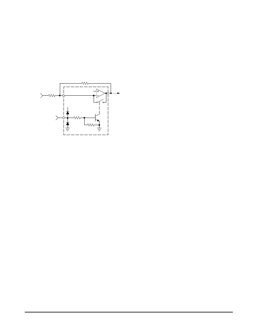
Figure 30. Microphone Amplifier and Mute
VCC
VB
RMI
From
Microphone
50 k
50 k
Mute
RMF
MCO
MCI
Receive Amplifier
The receive amplifier (Pins 16, 17) has the non–inverting
input internally connected to VB, while the inverting input and
the output are pinned out. Unlike most op amps, the amplifier
has an all NPN output stage, which maximizes phase margin
and gain–bandwidth. This feature ensures stability at gains
less than unity, as well as with a wide range of reactive loads.
The open loop gain is typically 70 dB (f < 100 Hz), and the
gain–bandwidth is typically 1.5 MHz. The maximum p–p
output swing for 1.0% or less distortion is shown in Figure 14.
The output impedance is <10
until current limiting is
reached (typically 2.0 mA peak). The input bias current at
RXI is typically 30 nA out of the pin.
Power Supply, VB and Chip Disable
The power supply voltage at Pin 24 is to be between 3.5
and 6.5 V for normal operation, and down to 2.7 V with the
AGC in effect (see AGC section). The supply current required
is typically 3.2 mA in the idle mode, and
≈
4.0 mA in the
transmit and receive modes. Figure 11 shows the supply
current for both the normal and disabled modes.
The output voltage at VB (Pin 6) is approximately equal to
(VCC – 0.7)/2, and provides an AC ground for the internal
amplifiers and the system. The output impedance at VB is
approximately 600
, and in conjunction with the external
capacitor at VB forms a low pass filter for power supply noise
rejection. The choice of the VB capacitor size is application
dependent based on whether the circuit is powered by the
telephone line or a regulated supply. See Figure 13 for
PSRR information. Since VB biases the microphone and
receive amplifiers, the amount of supply rejection at their
outputs is a function of the rejection at VB, as well as the
gains of the amplifiers.
The amount of current which can be sourced out of the VB
pin depends on the VCC voltage (see Figure 12). Drawing
current in excess of that shown in Figure 12 will cause VB to
drop low enough to disrupt the circuit’s operation. This pin
can sink
≈
100
μ
A when enabled, and 0
μ
A when disabled.
The Chip Disable (Pin 8) permits powering down the IC
for power conservation. With CD between 0 and 0.8 V,
normal operation is in effect. With CD between 2.0 V and
VCC, the IC is powered down, and the supply current drops
to about 110
μ
A (at VCC = 5.0 V, see Figure 11). When CD is
high, the microphone and receive amplifiers, the level
detectors, and the two attenuators are disabled (their
outputs go to a high impedance). The background noise
monitors are disabled, and Pins 3 and 10 will go to VCC. The
VB output, however, remains active, except that it cannot
sink any current.
The CD input must be kept within the range of VCC and
GND. See Figure 9 for input current requirements. If the input
is taken more than 0.4 V above VCC or below GND excessive
currents will flow, and the device’s operation will be distorted.
If the disable function is not used, the pin should be
connected to ground.
相关PDF资料 |
PDF描述 |
|---|---|
| MC33290D | ISO SERIAL LINK INTERFACE |
| MC33290 | ISO SERIAL LINK INTERFACE |
| MC33290DR2 | ISO SERIAL LINK INTERFACE |
| MC33290P | ISO SERIAL LINK INTERFACE |
| MC33304D | RAIL-TO-RAIL SLEEPMODE OPERATIONAL AMPLIFIER |
相关代理商/技术参数 |
参数描述 |
|---|---|
| MC33232D | 功能描述:功率因数校正 IC Critical Mode PFC RoHS:否 制造商:Fairchild Semiconductor 开关频率:300 KHz 最大功率耗散: 最大工作温度:+ 125 C 安装风格:SMD/SMT 封装 / 箱体:SOIC-8 封装:Reel |
| MC33232DG | 功能描述:功率因数校正 IC Critical Mode PFC RoHS:否 制造商:Fairchild Semiconductor 开关频率:300 KHz 最大功率耗散: 最大工作温度:+ 125 C 安装风格:SMD/SMT 封装 / 箱体:SOIC-8 封装:Reel |
| MC33232DR2 | 功能描述:功率因数校正 IC Critical Mode PFC RoHS:否 制造商:Fairchild Semiconductor 开关频率:300 KHz 最大功率耗散: 最大工作温度:+ 125 C 安装风格:SMD/SMT 封装 / 箱体:SOIC-8 封装:Reel |
| MC33232DR2G | 功能描述:功率因数校正 IC Critical Mode PFC RoHS:否 制造商:Fairchild Semiconductor 开关频率:300 KHz 最大功率耗散: 最大工作温度:+ 125 C 安装风格:SMD/SMT 封装 / 箱体:SOIC-8 封装:Reel |
| MC33232P | 功能描述:功率因数校正 IC Critical Mode PFC RoHS:否 制造商:Fairchild Semiconductor 开关频率:300 KHz 最大功率耗散: 最大工作温度:+ 125 C 安装风格:SMD/SMT 封装 / 箱体:SOIC-8 封装:Reel |
发布紧急采购,3分钟左右您将得到回复。