- 您现在的位置:买卖IC网 > PDF目录22208 > MC33260DR2 (ON Semiconductor)IC PFC COMPACT PRECONVERT 8SOIC PDF资料下载
参数资料
| 型号: | MC33260DR2 |
| 厂商: | ON Semiconductor |
| 文件页数: | 10/22页 |
| 文件大小: | 372K |
| 描述: | IC PFC COMPACT PRECONVERT 8SOIC |
| 产品变化通告: | LTB Notification 03/Jan/2008 |
| 标准包装: | 1 |
| 系列: | GreenLine™ |
| 模式: | 间歇导电(DCM) |
| 电流 - 启动: | 100µA |
| 电源电压: | 11 V ~ 16 V |
| 工作温度: | -40°C ~ 105°C |
| 安装类型: | 表面贴装 |
| 封装/外壳: | 8-SOIC(0.154",3.90mm 宽) |
| 供应商设备封装: | 8-SOICN |
| 包装: | 剪切带 (CT) |
| 其它名称: | MC33260DR2OSCT |
MC33260
http://onsemi.com
10
Pin Numbers are Relevant to the PDIP- -8 Version
R
o
=
r
V
o
u
regH
V
pin1
I
regH
Consequently:
In practice, V
pin1
is small compared to (V
o
)
regH
and this
equation can be simplified as follows (I
regH
being also
replaced by its typical value 200 mA):
R
o
H 5 ?/DIV>
r
V
o
u
regH
(k?
The regulation block output is connected to the Pin 2
through a 300 k?resistor. The Pin 2 voltage (V
control
) is
compared to the oscillator sawtooth for PWM control.
An external capacitor must be connected between Pin 2
andground,forexternalloopcompensation.Thebandwidth
is typically set below 20 Hz so that the regulation block
output should be relatively constant over a given ac line
cycle.Thisintegrationthatresultsinaconstanton- -timeover
the ac line period, prevents the mains frequency output
ripple from distorting the ac line current.
OSCILLATOR SECTION
The oscillator consists of three phases:
?nbsp Charge Phase: The oscillator capacitor voltage grows
up linearly from its bottom value (ground) until it
exceedsV
control
(regulation block output voltage). At
that moment, the PWM latch output gets low and the
oscillator discharge sequence is set.
?nbsp Discharge Phase: The oscillator capacitor is abruptly
discharged down to its valley value (0 V).
?nbsp Waiting Phase: At the end of the discharge sequence,
theoscillatorvoltageismaintainedinalowstateuntil
the PWM latch is set again.
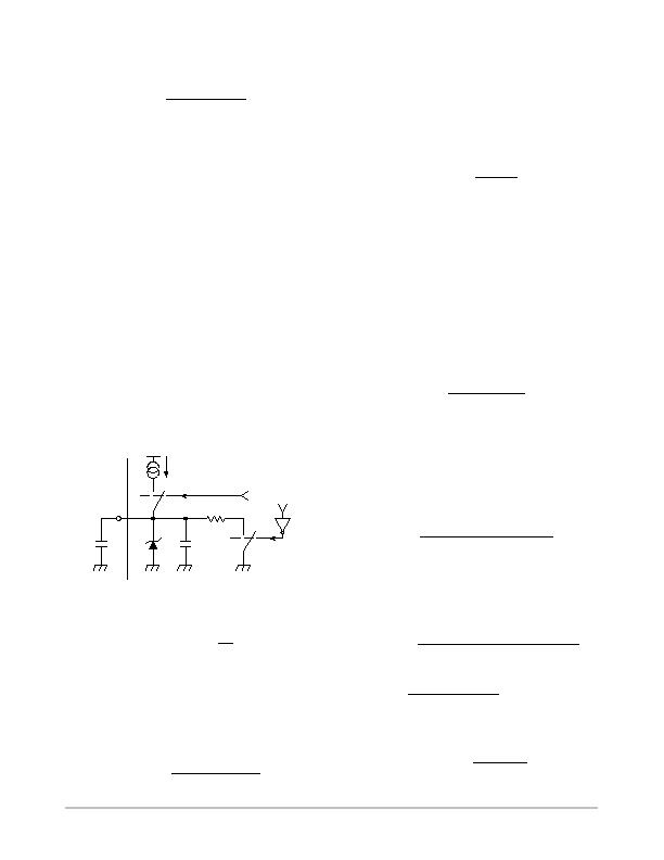
Figure 26. Oscillator
I
charge
= 2 ?I
o
?I
o
/ I
ref
0
1
CT
3
15 pF
0
1
Output_Ctrl
Theoscillatorchargecurrentisdependentonthefeedback
current (I
o
). In effect
I
charge
= 2 ?/DIV>
I
2
o
I
ref
where:
I
charge
is the oscillator charge current,
I
o
is the feedback current (drawn by Pin 1),
I
ref
is the internal reference current (200 mA).
So, the oscillator charge current is linked to the output
voltage level as follows:
I
charge
=
2 ?/DIV>
r
V
o
V
pin1
u
2
R
2
o
?I
ref
where:
V
o
is the output voltage,
R
o
is the feedback resistor,
V
pin1
is the Pin 1 clamp voltage.
Inpractice,V
pin1
thatisintherangeof2.5V,isverysmall
compared to V
o
. The equation can then be simplified by
neglecting V
pin1
:
I
charge
H
2 ?V
2
o
R
2
o
?I
ref
It must be noticed that the oscillator terminal (Pin 3) has
an internal capacitance (C
int
) that varies versus the Pin 3
voltage. Over the oscillator swing, its average value
typically equals 15 pF (min 10 pF, max 20 pF).
Thetotaloscillatorcapacitoristhenthesumoftheinternal
and external capacitors.
C
pin3
= C
T
+ C
int
PWM LATCH SECTION
The MC33260 operates in voltage mode: the regulation
block output (V
control
- - Pin 2 voltage) is compared to the
oscillator sawtooth so that the gate drive signal (Pin 7) is
high until the oscillator ramp exceeds V
control
.
The on- -time is then given by the following equation:
t
on
=
C
pin3
?V
control
I
ch
where:
t
on
is the on- -time,
C
pin3
is the total oscillator capacitor (sum of the
internal and external capacitor),
I
charge
is the oscillator charge current (Pin 3 current),
V
control
is the Pin 2 voltage (regulation block output).
Consequently,replacingI
charge
bytheexpressiongivenin
the Oscillator Section:
t
on
=
R
2
o
?I
ref
?C
pin3
?V
control
2 ?V
2
o
One can notice that the on- -time depends on V
o
(preconverter output voltage) and that the on- -time is
maximum when Vcontrol is maximum (1.5 V typically).
AtagivenV
o
,themaximumon- -timeisthenexpressedby
the following equation:
r
t
on
u
max =
C
pin3
?R
2
o
?I
ref
?/DIV>
r
V
control
u
max
2 ?V
2
o
This equation can be simplified replacing
`
2
[(
V
control
)
max
* I
ref
]
c
by K
osc
Refer to Electrical Characteristics, Oscillator Section.
Then:
r
t
on
u
max =
C
pin3
?R
2
o
K
osc
?V
2
o
相关PDF资料 |
PDF描述 |
|---|---|
| VF30100S-E3/4W | DIODE SCHOTTKY 30A 100V ITO220AB |
| VI-J0B-CX-F1 | CONVERTER MOD DC/DC 95V 75W |
| T95R476K020EZSL | CAP TANT 47UF 20V 10% 2824 |
| ESM06DREI | CONN EDGECARD 12POS .156 EYELET |
| VI-J04-CX-F4 | CONVERTER MOD DC/DC 48V 75W |
相关代理商/技术参数 |
参数描述 |
|---|---|
| MC33260DR2G | 功能描述:功率因数校正 IC Critical Conduction Mode PFC RoHS:否 制造商:Fairchild Semiconductor 开关频率:300 KHz 最大功率耗散: 最大工作温度:+ 125 C 安装风格:SMD/SMT 封装 / 箱体:SOIC-8 封装:Reel |
| MC33260P | 功能描述:功率因数校正 IC Critical Conduction RoHS:否 制造商:Fairchild Semiconductor 开关频率:300 KHz 最大功率耗散: 最大工作温度:+ 125 C 安装风格:SMD/SMT 封装 / 箱体:SOIC-8 封装:Reel |
| MC33260PG | 功能描述:功率因数校正 IC Critical Conduction Mode PFC RoHS:否 制造商:Fairchild Semiconductor 开关频率:300 KHz 最大功率耗散: 最大工作温度:+ 125 C 安装风格:SMD/SMT 封装 / 箱体:SOIC-8 封装:Reel |
| MC33261 | 制造商:SPC Multicomp 功能描述:HEATSINK TO220/218 16.7/W 制造商:SPC Multicomp 功能描述:HEATSINK TO220/218 16.7C/W 制造商:SPC Multicomp 功能描述:HEAT SINK; Packages Cooled:TO-218 / TO-220; Thermal Resistance:16.7C/W; External Height - Imperial:1"; External Height - Metric:25.4mm; External Width - Imperial:0.654"; External Width - Metric:16.6mm; Heat Sink Material:Aluminium ;RoHS Compliant: Yes |
| MC33261P | 制造商:Rochester Electronics LLC 功能描述:- Bulk |
发布紧急采购,3分钟左右您将得到回复。