- 您现在的位置:买卖IC网 > PDF目录359133 > MC33888FB (飞思卡尔半导体(中国)有限公司) Quad High Side and Octal Low Side Switch for Automotive Applications(4高端开关及8低端开关,用于自动应用) PDF资料下载
参数资料
| 型号: | MC33888FB |
| 厂商: | 飞思卡尔半导体(中国)有限公司 |
| 英文描述: | Quad High Side and Octal Low Side Switch for Automotive Applications(4高端开关及8低端开关,用于自动应用) |
| 中文描述: | 四高侧和汽车应用八路低边开关(4高端开关及8低端开关,用于自动应用) |
| 文件页数: | 14/18页 |
| 文件大小: | 711K |
| 代理商: | MC33888FB |
MC33888FB
SPI Interface and Protocol Description
Quad High Side and Octal Low Side Switch for Automotive
14
X : don
’
t care
NA Not Applicable
SO Communication
(see TABLE 3)
When the CSB pin is pulled low, the output status register for each output is loaded into the output register and the fault data is
clocked out MSB (OD15) first, as the new message data is clocked into the SI pin.
OD15 reflects the state of the watchdog bit (D15) that was addressed during the prior SOCR communication. If the OD15 is logic
L, then the following three MSBs (OD14, OD13, OD12) will reflect the logic states of the IHS0, IHS1 and FSI pins respectively. If
the OD15 bit is logic H, then the following three bits will reflect the logic states of the IHS2, IHS3 and WAKE pins respectively. The
next twelve bits clocked out of SO following a low transition of the CSB pin will reflect the state of each output, with a logic H in any
of the bits indicating that the respective output experienced a fault condition prior to the CSB transition. Any bits clocked out of the
SO pin after the first sixteen will be representative of the initial message bits that were clocked into the SI pin since the CSB pin first
transitioned to a logic L; this feature is useful for daisy chaining devices as well as message verification.
Following a CSB transition L to H, the device determines if the message was of a valid length (a valid message length is one that is
a multiple of 16 bits) and if so, latches the data into the appropriate registers. At this time, the SO pin is tri-stated and the fault
status register is now able to accept new fault status information.
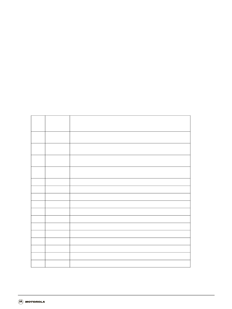
Table 3
SO OUTPUT BIT ASSIGNMENT
BIT
SIG
SO
MESSAGE
BIT
MESSAGE DISCRIPTION
MSB
OD15
Reflects the state of the Watchdog bit from the previously clocked in
message.
OD14
If OD15 is logic L, then this bit will reflect the state of the direct input IHS0. If
OD15 is logic H, then this bit will reflect the state of IHS2.
OD13
If OD15 is logic L, then this bit will reflect the state of the direct input IHS1. If
OD15 is logic H, then this bit will reflect the state of IHS3.
OD12
If OD15 is logic L, then this bit will reflect the state of the input FSI. If OD15 is
logic H, then this bit will reflect the state of the input WAKE.
OD11
Reports the absence or presence of a fault on LS11
OD10
Reports the absence or presence of a fault on LS10
OD9
Reports the absence or presence of a fault on LS9
OD8
Reports the absence or presence of a fault on LS8
OD7
Reports the absence or presence of a fault on LS7
OD6
Reports the absence or presence of a fault on LS6
OD5
Reports the absence or presence of a fault on LS5
OD4
Reports the absence or presence of a fault on LS4
OD3
Reports the absence or presence of a fault on HS3
OD2
Reports the absence or presence of a fault on HS2
OD1
Reports the absence or presence of a fault on HS1
LSB
OD0
Reports the absence or presence of a fault on HS0
F
Freescale Semiconductor, Inc.
For More Information On This Product,
n
.
相关PDF资料 |
PDF描述 |
|---|---|
| MC33889 | System Basis Chip (SBC) with Low Speed Fault Tolerant CAN Interface |
| MC33897 | Single-Wire CAN Transceiver(单线CAN收发器) |
| MC33972 | Multiple Switch Detection Interface with Suppressed Wake-Up(带抑制唤醒功能的多开关检测接口) |
| MC33976 | Dual Gauge Driver with Configurable Response Time(带可设置响应时间的双标尺驱动器) |
| MC33984 | Dual Intelligent High-Current Self-Protected Silicon High-Side Switch (4.0 mOhm)(双智能大电流带自保护功能的硅高端开关(4mOhm)) |
相关代理商/技术参数 |
参数描述 |
|---|---|
| MC33888FBR2 | 功能描述:电源开关 IC - 配电 QHSOLSS RoHS:否 制造商:Exar 输出端数量:1 开启电阻(最大值):85 mOhms 开启时间(最大值):400 us 关闭时间(最大值):20 us 工作电源电压:3.2 V to 6.5 V 电源电流(最大值): 最大工作温度:+ 85 C 安装风格:SMD/SMT 封装 / 箱体:SOT-23-5 |
| MC33888PNB | 制造商:FREESCALE-SEMI 功能描述: |
| MC33888PNBR2 | 制造商:FREESCALE-SEMI 功能描述: |
| MC33889BDW | 功能描述:网络控制器与处理器 IC SBC LIGHT PASS 3.3 RoHS:否 制造商:Micrel 产品:Controller Area Network (CAN) 收发器数量: 数据速率: 电源电流(最大值):595 mA 最大工作温度:+ 85 C 安装风格:SMD/SMT 封装 / 箱体:PBGA-400 封装:Tray |
| MC33889BDWR2 | 功能描述:网络控制器与处理器 IC SBC LIGHT PASS 3.3 RoHS:否 制造商:Micrel 产品:Controller Area Network (CAN) 收发器数量: 数据速率: 电源电流(最大值):595 mA 最大工作温度:+ 85 C 安装风格:SMD/SMT 封装 / 箱体:PBGA-400 封装:Tray |
发布紧急采购,3分钟左右您将得到回复。