参数资料
| 型号: | MC3423DR2 |
| 厂商: | ON Semiconductor |
| 文件页数: | 4/10页 |
| 文件大小: | 0K |
| 描述: | IC SENSOR UNDERVOLTAGE 8-SOIC |
| 产品变化通告: | LTB Notification 03/Jan/2008 |
| 标准包装: | 2,500 |
| 系列: | MC3423 |
| 技术: | 混合技术 |
| 电路数: | 2 |
| 应用: | 通用 |
| 封装/外壳: | 8-SOIC(0.154",3.90mm 宽) |
| 供应商设备封装: | 8-SOICN |
| 包装: | 带卷 (TR) |
�� �
�
�MC3423�
�APPLICATION� INFORMATION�
�Basic� Circuit� Configuration�
�The� basic� circuit� configuration� of� the� MC3423� OVP� is�
�shown� in� Figure� 3� for� supply� voltages� from� 4.5� V� to� 36� V,�
�and� in� Figure� 4� for� trip� voltages� above� 36� V.� The� threshold�
�(+� Sense�
�Lead)�
�1�
�+�
�or� trip� voltage� at� which� the� MC3423� will� trigger� and� supply�
�gate� drive� to� the� crowbar� SCR,� Q1,� is� determined� by� the�
�selection� of� R1� and� R2.� Their� values� can� be� determined� by�
�the� equation� given� in� Figures� 3� and� 4,� or� by� the� graph� shown�
�in� Figure� 8.� The� minimum� value� of� the� gate� current� limiting�
�resistor,� R� G� ,� is� given� in� Figure� 9.� Using� this� value� of� R� G� ,� the�
�SCR,� Q1,� will� receive� the� greatest� gate� current� possible�
�Power�
�Supply�
�Z1�
�R1�
�R2�
�2�
�5�
�1k�
�4� 3�
�MC3423�
�7�
�C�
�8� R� G�
�without� damaging� the� MC3423.� If� lower� output� currents�
�are� required,� R� G� can� be� increased� in� value.� The� switch,� S1,�
�shown� in� Figure� 3� may� be� used� to� reset� the� crowbar.�
�Otherwise,� the� power� supply,� across� which� the� SCR� is�
�connected,� must� be� shut� down� to� reset� the� crowbar.� If� a� non�
�current?limited� supply� is� used,� a� fuse� or� circuit� breaker,� F1,�
�should� be� used� to� protect� the� SCR� and/or� the� load.�
�The� circuit� configurations� shown� in� Figures� 3� and� 4� will�
�have� a� typical� propagating� delay� of� 1.0� m� s.� If� faster�
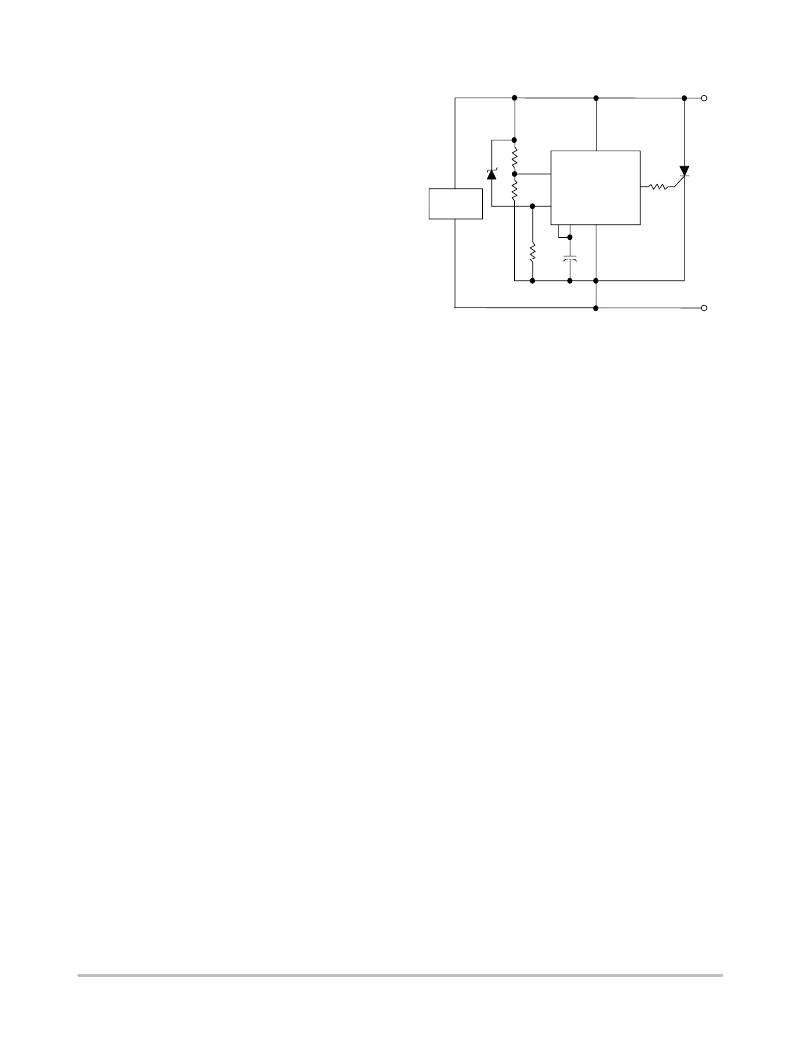
�(?� Sense� Lead)�
�Figure� 7.� Configuration� for� Programmable�
�Duration� of� Overvoltage� Condition� Before�
�Trip/With� Immediate� Trip� at�
�High� Overvoltages�
�?�
�operation� is� desired,� Pin� 3� may� be� connected� to� Pin� 2� with�
�Pin� 4� left� floating.� This� will� result� in� decreasing� the�
�propagating� delay� to� approximately� 0.5� m� s� at� the� expense�
�of� a� slightly� increased� TC� for� the� trip� voltage� value.�
�Configuration� for� Programmable� Minimum� Duration�
�of� Overvoltage� Condition� Before� Tripping�
�In� many� instances,� the� MC3423� OVP� will� be� used� in� a�
�noise� environment.� To� prevent� false� tripping� of� the� OVP�
�circuit� by� noise� which� would� not� normally� harm� the� load,�
�MC3423� has� a� programmable� delay� feature.� To� implement�
�this� feature,� the� circuit� configuration� of� Figure� 5� is� used.� In�
�this� configuration,� a� capacitor� is� connected� from� Pin� 3� to�
�V� EE� .� The� value� of� this� capacitor� determines� the� minimum�
�duration� of� the� overvoltage� condition� which� is� necessary� to�
�trip� the� OVP.� The� value� of� C� can� be� found� from� Figure� 10.�
�The� circuit� operates� in� the� following� manner:� When� V� CC�
�rises� above� the� trip� point� set� by� R1� and� R2,� an� internal�
�current� source� (Pin� 4)� begins� charging� the� capacitor,� C,�
�connected� to� Pin� 3.� If� the� overvoltage� condition� disappears�
�before� this� occurs,� the� capacitor� is� discharged� at� a� rate� ?� 10�
�times� faster� than� the� charging� rate,� resetting� the� timing�
�feature� until� the� next� overvoltage� condition� occurs.�
�Occasionally,� it� is� desired� that� immediate� crowbarring� of�
�the� supply� occur� when� a� high� overvoltage� condition� occurs,�
�while� retaining� the� false� tripping� immunity� of� Figure� 5.� In�
�this� case,� the� circuit� of� Figure� 6� can� be� used.� The� circuit� will�
�operate� as� previously� described� for� small� overvoltages,� but�
�will� immediately� trip� if� the� power� supply� voltage� exceeds�
�V� Z1� +� 1.4� V.�
�Additional� Features�
�1.� Activation� Indication� Output�
�An� additional� output� for� use� as� an� indicator� of� OVP�
�activation� is� provided� by� the� MC3423.� This� output� is� an�
�open� collector� transistor� which� saturates� when� the� OVP�
�is� activated.� In� addition,� it� can� be� used� to� clock� an� edge�
�triggered� flip?flop� whose� output� inhibits� or� shuts� down�
�the� power� supply� when� the� OVP� trips.� This� reduces� or�
�eliminates� the� heatsinking� requirements� for� the� crowbar�
�SCR.�
�2.� Remote� Activation� Input�
�Another� feature� of� the� MC3423� is� its� remote�
�activation� input,� Pin� 5.� If� the� voltage� on� this� CMOS/TTL�
�compatible� input� is� held� below� 0.8� V,� the� MC3423�
�operates� normally.� However,� if� it� is� raised� to� a� voltage�
�above� 2.0� V,� the� OVP� output� is� activated� independent� of�
�whether� or� not� an� overvoltage� condition� is� present.� It�
�should� be� noted� that� Pin� 5� has� an� internal� pullup� current�
�source.� This� feature� can� be� used� to� accomplish� an�
�orderly� and� sequenced� shutdown� of� system� power�
�supplies� during� a� system� fault� condition.� In� addition,� the�
�activation� indication� output� of� one� MC3423� can� be� used�
�to� activate� another� MC3423� if� a� single� transistor� inverter�
�is� used� to� interface� the� former� ’s� indication� output� to� the�
�latter� ’s� remote� activation� input,� as� shown� in� Figure� 7.� In�
�this� circuit,� the� indication� output� (Pin� 6)� of� the� MC3423�
�on� power� supply� 1� is� used� to� activate� the� MC3423�
�associated� with� power� supply� 2.� Q1� is� any� small� PNP�
�with� adequate� voltage� rating.�
�http://onsemi.com�
�4�
�相关PDF资料 |
PDF描述 |
|---|---|
| 8020.0603 | FUSE 12A 250VAC 6X32 SLOW |
| LTC6101AIMS8#TRPBF | IC AMP CURRENT SENSE 8-MSOP |
| 0001.2711.11 | FUSE 5A 250V 5X20 T-LAG SMD |
| AD8130ARZ-REEL7 | IC AMP DIFF LN LDIST 40MA 8SOIC |
| 0001.2710.11 | FUSE 4A 250V 5X20 T-LAG SMD |
相关代理商/技术参数 |
参数描述 |
|---|---|
| MC3423DR2G | 功能描述:监控电路 6.5V OverVoltage Crowbar Sensing RoHS:否 制造商:STMicroelectronics 监测电压数: 监测电压: 欠电压阈值: 过电压阈值: 输出类型:Active Low, Open Drain 人工复位:Resettable 监视器:No Watchdog 电池备用开关:No Backup 上电复位延迟(典型值):10 s 电源电压-最大:5.5 V 最大工作温度:+ 85 C 安装风格:SMD/SMT 封装 / 箱体:UDFN-6 封装:Reel |
| MC3423P | 制造商:Motorola Inc 功能描述: |
| MC3423P1 | 功能描述:监控电路 6.5V OverVoltage RoHS:否 制造商:STMicroelectronics 监测电压数: 监测电压: 欠电压阈值: 过电压阈值: 输出类型:Active Low, Open Drain 人工复位:Resettable 监视器:No Watchdog 电池备用开关:No Backup 上电复位延迟(典型值):10 s 电源电压-最大:5.5 V 最大工作温度:+ 85 C 安装风格:SMD/SMT 封装 / 箱体:UDFN-6 封装:Reel |
| MC3423P1G | 功能描述:监控电路 6.5V OverVoltage Crowbar Sensing RoHS:否 制造商:STMicroelectronics 监测电压数: 监测电压: 欠电压阈值: 过电压阈值: 输出类型:Active Low, Open Drain 人工复位:Resettable 监视器:No Watchdog 电池备用开关:No Backup 上电复位延迟(典型值):10 s 电源电压-最大:5.5 V 最大工作温度:+ 85 C 安装风格:SMD/SMT 封装 / 箱体:UDFN-6 封装:Reel |
| MC3423P1G | 制造商:ON Semiconductor 功能描述:Voltage Regulator IC Voltage Regulator T |
发布紧急采购,3分钟左右您将得到回复。