- 您现在的位置:买卖IC网 > PDF目录1948 > MC56F8322VFAE (Freescale Semiconductor)IC DSP 16BIT 60MHZ 48-LQFP PDF资料下载
参数资料
| 型号: | MC56F8322VFAE |
| 厂商: | Freescale Semiconductor |
| 文件页数: | 122/136页 |
| 文件大小: | 0K |
| 描述: | IC DSP 16BIT 60MHZ 48-LQFP |
| 标准包装: | 250 |
| 系列: | 56F8xxx |
| 核心处理器: | 56800E |
| 芯体尺寸: | 16-位 |
| 速度: | 60MHz |
| 连通性: | CAN,SCI,SPI |
| 外围设备: | POR,PWM,温度传感器,WDT |
| 输入/输出数: | 21 |
| 程序存储器容量: | 40KB(20K x 16) |
| 程序存储器类型: | 闪存 |
| RAM 容量: | 6K x 16 |
| 电压 - 电源 (Vcc/Vdd): | 2.25 V ~ 3.6 V |
| 数据转换器: | A/D 6x12b |
| 振荡器型: | 内部 |
| 工作温度: | -40°C ~ 105°C |
| 封装/外壳: | 48-LQFP |
| 包装: | 托盘 |
| 配用: | MC56F8323EVME-ND - BOARD EVALUATION MC56F8323 |
第1页第2页第3页第4页第5页第6页第7页第8页第9页第10页第11页第12页第13页第14页第15页第16页第17页第18页第19页第20页第21页第22页第23页第24页第25页第26页第27页第28页第29页第30页第31页第32页第33页第34页第35页第36页第37页第38页第39页第40页第41页第42页第43页第44页第45页第46页第47页第48页第49页第50页第51页第52页第53页第54页第55页第56页第57页第58页第59页第60页第61页第62页第63页第64页第65页第66页第67页第68页第69页第70页第71页第72页第73页第74页第75页第76页第77页第78页第79页第80页第81页第82页第83页第84页第85页第86页第87页第88页第89页第90页第91页第92页第93页第94页第95页第96页第97页第98页第99页第100页第101页第102页第103页第104页第105页第106页第107页第108页第109页第110页第111页第112页第113页第114页第115页第116页第117页第118页第119页第120页第121页当前第122页第123页第124页第125页第126页第127页第128页第129页第130页第131页第132页第133页第134页第135页第136页
56F8322 Techncial Data, Rev. 16
86
Freescale Semiconductor
Preliminary
6.5.6.3
IRQ—Bit 10
This bit controls the pull-up resistors on the IRQA pin.
6.5.6.4
Reserved—Bits 9–4
This bit field is reserved or not implemented. It is read as 0 and cannot be modified by writing.
6.5.6.5
JTAG—Bit 3
This bit controls the pull-up resistors on the TRST (This pin is always tied inactive on the 56F8322), TMS
and TDI pins.
6.5.6.6
Reserved—Bits 2–0
This bit field is reserved or not implemented. It is read as 0 and cannot be modified by writing.
6.5.7
CLKO Select Register (SIM_CLKOSR)
The CLKO select register can be used to multiplex out any one of the clocks generated inside the clock
generation and SIM modules. The default value is SYS_CLK. All other clocks primarily muxed out are
for test purposes only, and are subject to significant unspecified latencies at high frequencies.
The upper four bits of the GPIOB register can function as GPIO, Quad Decoder #0 signals, or as additional
clock output signals. GPIO has priority and is enabled/disabled via the GPIOB_PER. If GPIOB[7:4] are
programmed to operate as peripheral outputs, then the choice between Quad Decoder #0 and additional
clock outputs is made here in the CLKOSR. The default state is for the peripheral function of GPIOB[7:4]
to be programmed as Quad Decoder #0. This can be changed by altering PHASE0 through INDEX as
shown in Figure 6-9.
The CLKOUT pin is not bonded out in this device. Instead, it is offered only as a pad for die-level testing.
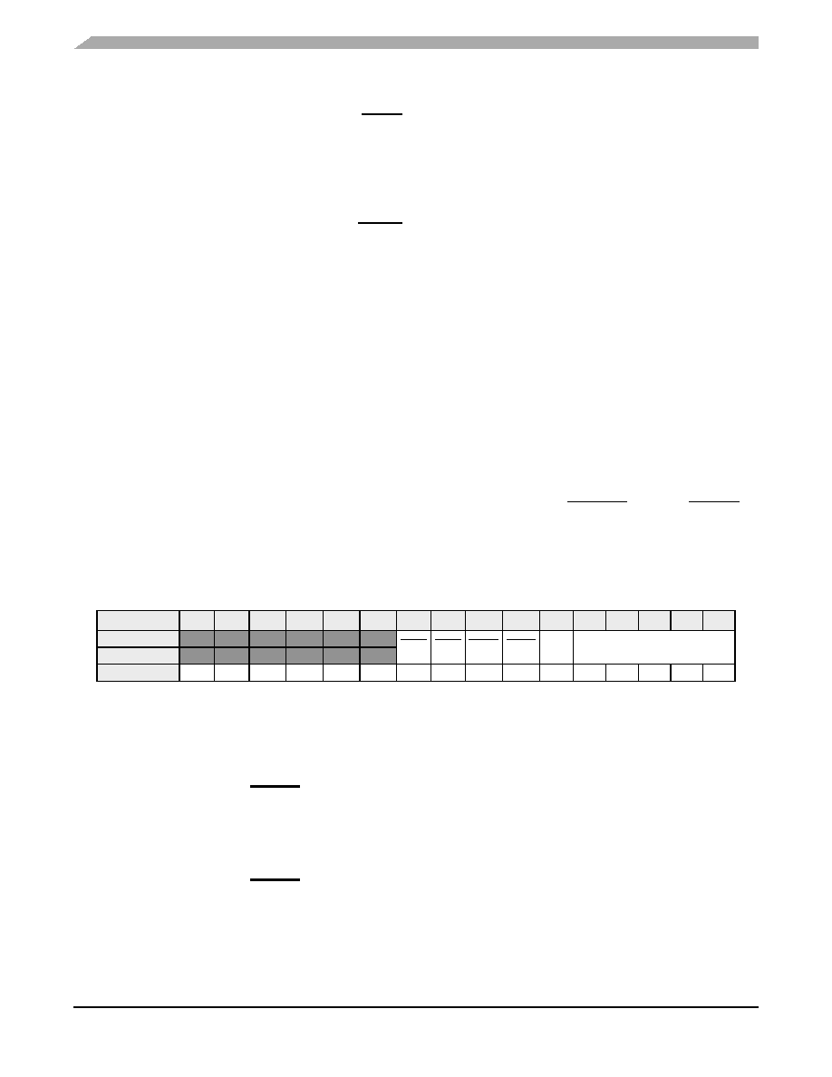
Figure 6-9 CLKO Select Register (SIM_CLKOSR)
6.5.7.1
Reserved—Bits 15–10
This bit field is reserved or not implemented. It is read as 0 and cannot be modified by writing.
6.5.7.2
PHASEA0 (PHSA)—Bit 9
0 = Peripheral output function of GPIOB[7] is defined to be PHASEA0
1 = Peripheral output function of GPI B[7] is defined to be the oscillator clock (MSTR_OSC, see
6.5.7.3
PHASEB0 (PHSB)—Bit 8
0 = Peripheral output function of GPIOB[6] is defined to be PHASEB0
1 = Peripheral output function of GPIOB[6] is defined to be SYS_CLK2
Base + $A
15
14
13
12
11
10
9
8
7
6
5
4
3
2
1
0
Read
0
PHSA PHSB INDEX HOME
CLK
DIS
CLKOSEL
Write
RESET
0
000
0
1
0
相关PDF资料 |
PDF描述 |
|---|---|
| MC56F8323VFBE | IC MPU HYBRID DSP 32K 64-LQFP |
| MC56F8335VFGE | IC DIGITAL SIGNAL CTLR 128-LQFP |
| MC56F8345MFGE | IC DSP 16BIT 60MHZ 128-LQFP |
| MC56F8346VFVE | IC DSP 16BIT 60MHZ 144-LQFP |
| MC56F8366VFVE | IC DSP 16BIT 60MHZ 144-LQFP |
相关代理商/技术参数 |
参数描述 |
|---|---|
| MC56F8322VFAER2 | 功能描述:数字信号处理器和控制器 - DSP, DSC 16 BIT HYBRID CNTRLR RoHS:否 制造商:Microchip Technology 核心:dsPIC 数据总线宽度:16 bit 程序存储器大小:16 KB 数据 RAM 大小:2 KB 最大时钟频率:40 MHz 可编程输入/输出端数量:35 定时器数量:3 设备每秒兆指令数:50 MIPs 工作电源电压:3.3 V 最大工作温度:+ 85 C 封装 / 箱体:TQFP-44 安装风格:SMD/SMT |
| MC56F8323 | 制造商:FREESCALE 制造商全称:Freescale Semiconductor, Inc 功能描述:16-bit Digital Signal Controllers |
| MC56F8323EVM | 功能描述:开发板和工具包 - 其他处理器 MC56F832X Dev Kit RoHS:否 制造商:Freescale Semiconductor 产品:Development Systems 工具用于评估:P3041 核心:e500mc 接口类型:I2C, SPI, USB 工作电源电压: |
| MC56F8323EVM | 制造商:Freescale Semiconductor 功能描述:Tools Development kit Kit Con |
| MC56F8323EVME | 功能描述:开发板和工具包 - 其他处理器 MC56F8323 EVAL BRD RoHS:否 制造商:Freescale Semiconductor 产品:Development Systems 工具用于评估:P3041 核心:e500mc 接口类型:I2C, SPI, USB 工作电源电压: |
发布紧急采购,3分钟左右您将得到回复。