- 您现在的位置:买卖IC网 > PDF目录45236 > MC68HC705JJ7CP (FREESCALE SEMICONDUCTOR INC) 8-BIT, OTPROM, 2.1 MHz, MICROCONTROLLER, PDIP20 PDF资料下载
参数资料
| 型号: | MC68HC705JJ7CP |
| 厂商: | FREESCALE SEMICONDUCTOR INC |
| 元件分类: | 微控制器/微处理器 |
| 英文描述: | 8-BIT, OTPROM, 2.1 MHz, MICROCONTROLLER, PDIP20 |
| 封装: | PLASTIC, DIP-20 |
| 文件页数: | 122/164页 |
| 文件大小: | 1165K |
| 代理商: | MC68HC705JJ7CP |
第1页第2页第3页第4页第5页第6页第7页第8页第9页第10页第11页第12页第13页第14页第15页第16页第17页第18页第19页第20页第21页第22页第23页第24页第25页第26页第27页第28页第29页第30页第31页第32页第33页第34页第35页第36页第37页第38页第39页第40页第41页第42页第43页第44页第45页第46页第47页第48页第49页第50页第51页第52页第53页第54页第55页第56页第57页第58页第59页第60页第61页第62页第63页第64页第65页第66页第67页第68页第69页第70页第71页第72页第73页第74页第75页第76页第77页第78页第79页第80页第81页第82页第83页第84页第85页第86页第87页第88页第89页第90页第91页第92页第93页第94页第95页第96页第97页第98页第99页第100页第101页第102页第103页第104页第105页第106页第107页第108页第109页第110页第111页第112页第113页第114页第115页第116页第117页第118页第119页第120页第121页当前第122页第123页第124页第125页第126页第127页第128页第129页第130页第131页第132页第133页第134页第135页第136页第137页第138页第139页第140页第141页第142页第143页第144页第145页第146页第147页第148页第149页第150页第151页第152页第153页第154页第155页第156页第157页第158页第159页第160页第161页第162页第163页第164页
Parallel Input/Output
MC68HC705JJ7 MC68HC705JP7 Advance Information Data Sheet, Rev. 4.1
60
Freescale Semiconductor
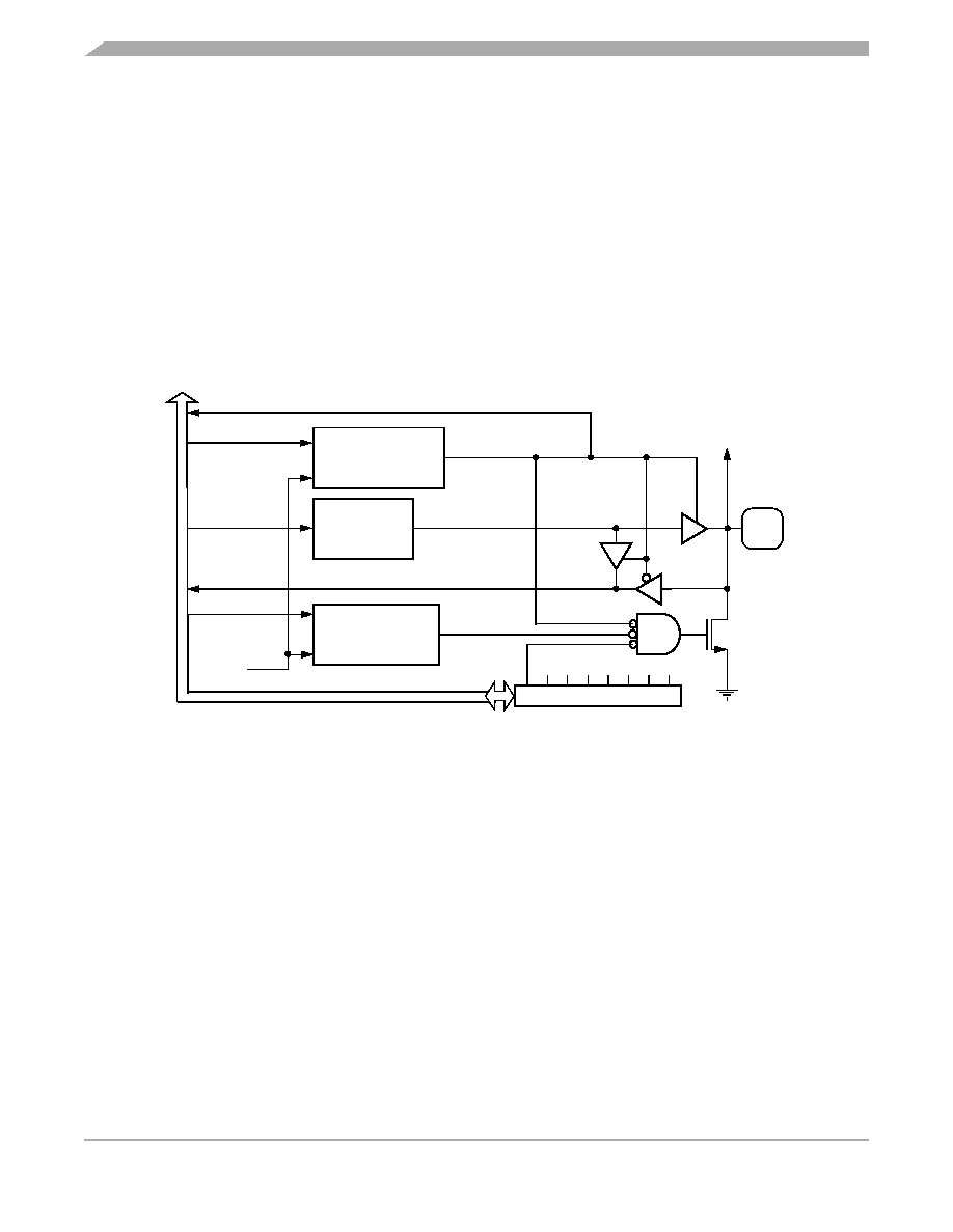
7.3.4 Port B Logic
All port B pins have the general I/O port logic similar to port A; but they also share this function with inputs
or outputs from other modules, which are also attached to the pin itself or override the general I/O
function. PB0, PB1, PB2, and PB3 simply share their inputs with another module. PB4, PB5, PB6, and
PB7 will have their operation altered by outputs or controls from other modules.
7.3.5 PB0, PBI, PB2, and PB3 Logic
The typical I/O logic shown in Figure 7-8 is used for PB0, PB1, PB2, and PB3 pins of port B. When these
port B pins are programmed as an output, reading the port bit actually reads the value of the data latch
and not the voltage on the pin itself. When these port B pins are programmed as an input, reading the port
bit reads the voltage level on the pin. The data latch can always be written, regardless of the state of its
DDRB bit. The operations of the PB0–PB3 pins are summarized in Table 7-2.
Figure 7-8. PB0–PB3 Pin I/O Circuit
The PB0–PB3 pins share their inputs with another module. When using the other attached module, these
conditions must be observed:
1.
If the DDRB configures the pin as an output, then the port data register can provide an output which
may conflict with any external input source to the other module. The pulldown device will be
disabled in this case.
2.
If the DDRB configures the pin as an input, then reading the port data register will return the state
of the input in terms of the digital threshold for that pin (analog inputs will default to logic states).
3.
If DDRB configures the pin as an input and the pulldown device is activated for a pin, it will also
load the input to the other module.
4.
If interaction between the port logic and the other module is not desired, the pin should be
configured as an input by clearing the appropriate DDRB bit. The input pulldown device is disabled
by clearing the appropriate PDRB bit (or by disabling programmable pulldowns with the SWPDI bit
in the MOR).
PORT BDATA
REGISTER
BIT PBx
DATA DIRECTION
REGISTER B
BIT DDRBx
PULLDOWN
REGISTER B
BIT PDIBx
R
PBx
ANALOG SUBSYSTEM,
AND PROGRAMMABLE
TIMER INPUT CAPTURE
READ $0005
WRITE $0001
READ $0001
WRITE $0011
PULLDOWN
DEVICE
RESET
INTERNA
LD
AT
A
B
U
S
(PINS PB0, PB1, PB2, PB3)
WRITE $0005
SWPDI
MASK OPTION REG. ($1FF1)
相关PDF资料 |
PDF描述 |
|---|---|
| MC68HC705JJ7S | 8-BIT, UVPROM, 2.1 MHz, MICROCONTROLLER, CDIP20 |
| MC68HC705K1DWR2 | 8-BIT, OTPROM, MICROCONTROLLER, PDSO16 |
| MC68HC705K1CP | 8-BIT, OTPROM, MICROCONTROLLER, PDIP16 |
| MC68HC705K1P | 8-BIT, OTPROM, 2 MHz, MICROCONTROLLER, PDIP16 |
| MC68HC705K1DW | 8-BIT, OTPROM, MICROCONTROLLER, PDSO16 |
相关代理商/技术参数 |
参数描述 |
|---|---|
| MC68HC705JP7CDW | 功能描述:IC MCU 8BIT 28-SOIC RoHS:否 类别:集成电路 (IC) >> 嵌入式 - 微控制器, 系列:HC05 其它有关文件:STM32F101T8 View All Specifications 特色产品:STM32 32-bit Cortex MCUs 标准包装:490 系列:STM32 F1 核心处理器:ARM? Cortex?-M3 芯体尺寸:32-位 速度:36MHz 连通性:I²C,IrDA,LIN,SPI,UART/USART 外围设备:DMA,PDR,POR,PVD,PWM,温度传感器,WDT 输入/输出数:26 程序存储器容量:64KB(64K x 8) 程序存储器类型:闪存 EEPROM 大小:- RAM 容量:10K x 8 电压 - 电源 (Vcc/Vdd):2 V ~ 3.6 V 数据转换器:A/D 10x12b 振荡器型:内部 工作温度:-40°C ~ 85°C 封装/外壳:36-VFQFN,36-VFQFPN 包装:托盘 配用:497-10030-ND - STARTER KIT FOR STM32497-8853-ND - BOARD DEMO STM32 UNIV USB-UUSCIKSDKSTM32-PL-ND - KIT IAR KICKSTART STM32 CORTEXM3497-8512-ND - KIT STARTER FOR STM32F10XE MCU497-8505-ND - KIT STARTER FOR STM32F10XE MCU497-8304-ND - KIT STM32 MOTOR DRIVER BLDC497-6438-ND - BOARD EVALUTION FOR STM32 512K497-6289-ND - KIT PERFORMANCE STICK FOR STM32MCBSTM32UME-ND - BOARD EVAL MCBSTM32 + ULINK-MEMCBSTM32U-ND - BOARD EVAL MCBSTM32 + ULINK2更多... 其它名称:497-9032STM32F101T8U6-ND |
| MC68HC705JP7CP | 制造商:Rochester Electronics LLC 功能描述: 制造商:Freescale Semiconductor 功能描述: |
| MC68HC705K1CDW | 制造商:Motorola Inc 功能描述: |
| MC68HC705KJ1CDW | 功能描述:8位微控制器 -MCU 8 Bit 4MHz RoHS:否 制造商:Silicon Labs 核心:8051 处理器系列:C8051F39x 数据总线宽度:8 bit 最大时钟频率:50 MHz 程序存储器大小:16 KB 数据 RAM 大小:1 KB 片上 ADC:Yes 工作电源电压:1.8 V to 3.6 V 工作温度范围:- 40 C to + 105 C 封装 / 箱体:QFN-20 安装风格:SMD/SMT |
| MC68HC705KJ1CP | 功能描述:IC MCU 4MHZ 1.2K OTP 16-DIP RoHS:否 类别:集成电路 (IC) >> 嵌入式 - 微控制器, 系列:HC05 其它有关文件:STM32F101T8 View All Specifications 特色产品:STM32 32-bit Cortex MCUs 标准包装:490 系列:STM32 F1 核心处理器:ARM? Cortex?-M3 芯体尺寸:32-位 速度:36MHz 连通性:I²C,IrDA,LIN,SPI,UART/USART 外围设备:DMA,PDR,POR,PVD,PWM,温度传感器,WDT 输入/输出数:26 程序存储器容量:64KB(64K x 8) 程序存储器类型:闪存 EEPROM 大小:- RAM 容量:10K x 8 电压 - 电源 (Vcc/Vdd):2 V ~ 3.6 V 数据转换器:A/D 10x12b 振荡器型:内部 工作温度:-40°C ~ 85°C 封装/外壳:36-VFQFN,36-VFQFPN 包装:托盘 配用:497-10030-ND - STARTER KIT FOR STM32497-8853-ND - BOARD DEMO STM32 UNIV USB-UUSCIKSDKSTM32-PL-ND - KIT IAR KICKSTART STM32 CORTEXM3497-8512-ND - KIT STARTER FOR STM32F10XE MCU497-8505-ND - KIT STARTER FOR STM32F10XE MCU497-8304-ND - KIT STM32 MOTOR DRIVER BLDC497-6438-ND - BOARD EVALUTION FOR STM32 512K497-6289-ND - KIT PERFORMANCE STICK FOR STM32MCBSTM32UME-ND - BOARD EVAL MCBSTM32 + ULINK-MEMCBSTM32U-ND - BOARD EVAL MCBSTM32 + ULINK2更多... 其它名称:497-9032STM32F101T8U6-ND |
发布紧急采购,3分钟左右您将得到回复。