- 您现在的位置:买卖IC网 > PDF目录1949 > MC68HC705SR3CPE (Freescale Semiconductor)IC MCU 3.75K 2.1MHZ OTP 40-DIP PDF资料下载
参数资料
| 型号: | MC68HC705SR3CPE |
| 厂商: | Freescale Semiconductor |
| 文件页数: | 15/96页 |
| 文件大小: | 0K |
| 描述: | IC MCU 3.75K 2.1MHZ OTP 40-DIP |
| 标准包装: | 9 |
| 系列: | HC05 |
| 核心处理器: | HC05 |
| 芯体尺寸: | 8-位 |
| 速度: | 4MHz |
| 外围设备: | LED,POR |
| 输入/输出数: | 32 |
| 程序存储器容量: | 3.75KB(3.75K x 8) |
| 程序存储器类型: | OTP |
| RAM 容量: | 192 x 8 |
| 电压 - 电源 (Vcc/Vdd): | 3 V ~ 5.5 V |
| 数据转换器: | A/D 4x8b |
| 振荡器型: | 内部 |
| 工作温度: | -40°C ~ 85°C |
| 封装/外壳: | 40-DIP(0.600",15.24mm) |
| 包装: | 管件 |
第1页第2页第3页第4页第5页第6页第7页第8页第9页第10页第11页第12页第13页第14页当前第15页第16页第17页第18页第19页第20页第21页第22页第23页第24页第25页第26页第27页第28页第29页第30页第31页第32页第33页第34页第35页第36页第37页第38页第39页第40页第41页第42页第43页第44页第45页第46页第47页第48页第49页第50页第51页第52页第53页第54页第55页第56页第57页第58页第59页第60页第61页第62页第63页第64页第65页第66页第67页第68页第69页第70页第71页第72页第73页第74页第75页第76页第77页第78页第79页第80页第81页第82页第83页第84页第85页第86页第87页第88页第89页第90页第91页第92页第93页第94页第95页第96页
Freescale
2-2
MC68HC05SR3
PIN DESCRIPTIONS
2
2.2
OSC1 and OSC2 Connections
The OSC1 and OSC2 pins are the connections for the on-chip oscillator — the following
configurations are available:
1) A crystal or ceramic resonator as shown in Figure 2-1(a).
2) An external clock signal as shown in Figure 2-1(b).
3) RC options as shown in Figure 2-1(c) and Figure 2-1(d).
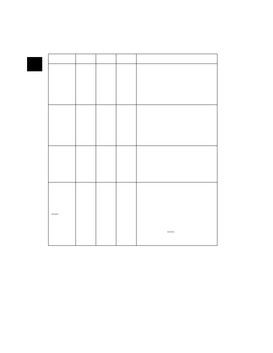
PA0-PA7
33-40
34-41
42-44, 1-5
These eight I/O lines comprise port A. The state of any pin
is software programmable. All port A lines are configured as
input during power-on or external reset.
PA0-PA7 are also associated with the Keyboard Interrupt
function. Each pin is equipped with a programmable
integrated 20K pull-up resistor connected to VDD when
configured as input. When programmed as output, each pin
can provide a current drive of 10mA. See Section 3 for
details on the I/O ports.
PB0-PB7
25-32
26-33
31, 35-41
These eight I/O lines comprise port B. The state of any pin
is software programmable. All port B lines are configured as
input during power-on or external reset.
Each pin is equipped with a programmable integrated 20K
pull-up resistor connected to VDD when configured as input.
When programmed as output, each pin can provide a
current drive of 10mA. PB5-PB7 can also be programmed to
provide a lower current drive of 2mA. See Section 3 for
details on the I/O ports.
PC0-PC7
9-16
10-17
15-22
These eight I/O lines comprise port C. The state of any pin
is software programmable. All port C lines are configured as
input during power-on or external reset.
Each pin is equipped with a programmable integrated 20K
pull-up resistor connected to VDD when configured as input.
When programmed as output, each pin can provide a
current drive of 10mA. See Section 3 for details on the I/O
ports.
PD0-PD7
AN0-AN3
IRQ2
VRH
VRL
24-21, 20-17
24-21
18
19
20
25-22, 21-18
25-22
19
20
21
30-23
30-27
24
25
26
These eight I/O lines comprise port D. The state of any pin
is software programmable. All port D lines are configured as
input during power-on or external reset.
Each pin is equipped with a programmable integrated 20K
pull-up resistor connected to VDD when configured as input.
When programmed as output, each pin can provide a
current drive of 10mA.
PD0-PD3 become analog inputs AN0-AN3 when the ADON
bit is set in the ADC Status and Control Register ($0E). PD4
and PD5 becomes VRL and VRH respectively for the ADC
reference voltage inputs.
PD6 is configured as IRQ2 by setting IRQ2E in the
Miscellaneous Control Register ($0C).
See Section 3 for details on the I/O ports.
PIN NAME
40-pin PDIP
PIN No.
42-pin SDIP
PIN No.
44-pin QFP
PIN No.
DESCRIPTION
TPG
20
05SR3.Book Page 2 Thursday, August 4, 2005 1:08 PM
相关PDF资料 |
PDF描述 |
|---|---|
| MC68HC711D3CFN2 | IC MCU 2MHZ 4K OTP 44-PLCC |
| MC68HC908GT8CFB | IC MCU 8K FLASH 8MHZ 44-QFP |
| MC68HC908JL3ECFA | IC MCU 4K FLASH 8MHZ 48-LQFP |
| MC68HC908QT2CFQ | MCU 8-BIT 1.5KB FLASH 8-DFN |
| MC68HC908SR12CFA | MICROCONTROLLER 48 PIN |
相关代理商/技术参数 |
参数描述 |
|---|---|
| MC68HC705SR3CPE | 制造商:Freescale Semiconductor 功能描述:8-Bit Microcontroller IC |
| MC68HC705SR3PE | 功能描述:IC MCU 3.75K 2.1MHZ OTP 40-DIP RoHS:是 类别:集成电路 (IC) >> 嵌入式 - 微控制器, 系列:HC05 标准包装:1 系列:AVR® ATmega 核心处理器:AVR 芯体尺寸:8-位 速度:16MHz 连通性:I²C,SPI,UART/USART 外围设备:欠压检测/复位,POR,PWM,WDT 输入/输出数:32 程序存储器容量:32KB(16K x 16) 程序存储器类型:闪存 EEPROM 大小:1K x 8 RAM 容量:2K x 8 电压 - 电源 (Vcc/Vdd):2.7 V ~ 5.5 V 数据转换器:A/D 8x10b 振荡器型:内部 工作温度:-40°C ~ 125°C 封装/外壳:44-TQFP 包装:剪切带 (CT) 其它名称:ATMEGA324P-B15AZCT |
| MC68HC706P6ACDW | 制造商:Motorola Inc 功能描述: |
| MC68HC708MP16CFU | 制造商:MAJOR 功能描述: |
| MC68HC711D3CFBE2 | 制造商:Freescale Semiconductor 功能描述: |
发布紧急采购,3分钟左右您将得到回复。