- 您现在的位置:买卖IC网 > PDF目录80570 > MC68LK332GCFC16 (MOTOROLA INC) 32-BIT, 16.78 MHz, MICROCONTROLLER, PQFP132 PDF资料下载
参数资料
| 型号: | MC68LK332GCFC16 |
| 厂商: | MOTOROLA INC |
| 元件分类: | 微控制器/微处理器 |
| 英文描述: | 32-BIT, 16.78 MHz, MICROCONTROLLER, PQFP132 |
| 封装: | PLASTIC, QFP-132 |
| 文件页数: | 32/111页 |
| 文件大小: | 650K |
| 代理商: | MC68LK332GCFC16 |
第1页第2页第3页第4页第5页第6页第7页第8页第9页第10页第11页第12页第13页第14页第15页第16页第17页第18页第19页第20页第21页第22页第23页第24页第25页第26页第27页第28页第29页第30页第31页当前第32页第33页第34页第35页第36页第37页第38页第39页第40页第41页第42页第43页第44页第45页第46页第47页第48页第49页第50页第51页第52页第53页第54页第55页第56页第57页第58页第59页第60页第61页第62页第63页第64页第65页第66页第67页第68页第69页第70页第71页第72页第73页第74页第75页第76页第77页第78页第79页第80页第81页第82页第83页第84页第85页第86页第87页第88页第89页第90页第91页第92页第93页第94页第95页第96页第97页第98页第99页第100页第101页第102页第103页第104页第105页第106页第107页第108页第109页第110页第111页
MC68332
MOTOROLA
MC68332TS/D
27
3.4.3 Address Bus
Address bus signals ADDR[23:0] define the address of the most significant byte to be transferred during
a bus cycle. The MCU places the address on the bus at the beginning of a bus cycle. The address is
valid while AS is asserted.
3.4.4 Address Strobe
AS is a timing signal that indicates the validity of an address on the address bus and the validity of many
control signals. It is asserted one-half clock after the beginning of a bus cycle.
3.4.5 Data Bus
Data bus signals DATA[15:0] make up a bidirectional, non-multiplexed parallel bus that transfers data
to or from the MCU. A read or write operation can transfer 8 or 16 bits of data in one bus cycle. During
a read cycle, the data is latched by the MCU on the last falling edge of the clock for that bus cycle. For
a write cycle, all 16 bits of the data bus are driven, regardless of the port width or operand size. The
MCU places the data on the data bus one-half clock cycle after AS is asserted in a write cycle.
3.4.6 Data Strobe
Data strobe (DS) is a timing signal. For a read cycle, the MCU asserts DS to signal an external device
to place data on the bus. DS is asserted at the same time as AS during a read cycle. For a write cycle,
DS signals an external device that data on the bus is valid. The MCU asserts DS one full clock cycle
after the assertion of AS during a write cycle.
3.4.7 Bus Cycle Termination Signals
During bus cycles, external devices assert the data transfer and size acknowledge signals (DSACK1
and DSACK0). During a read cycle, the signals tell the MCU to terminate the bus cycle and to latch data.
During a write cycle, the signals indicate that an external device has successfully stored data and that
the cycle can end. These signals also indicate to the MCU the size of the port for the bus cycle just com-
pleted. (Refer to 3.4.9 Dynamic Bus Sizing.)
The bus error (BERR) signal is also a bus cycle termination indicator and can be used in the absence
of DSACK1 and DSACK0 to indicate a bus error condition. It can also be asserted in conjunction with
these signals, provided it meets the appropriate timing requirements. The internal bus monitor can be
used to generate the BERR signal for internal and internal-to-external transfers. When BERR and HALT
are asserted simultaneously, the CPU takes a bus error exception.
Autovector signal (AVEC) can terminate external IRQ pin interrupt acknowledge cycles. AVEC indicates
that the MCU will internally generate a vector number to locate an interrupt handler routine. If it is con-
tinuously asserted, autovectors will be generated for all external interrupt requests. AVEC is ignored
during all other bus cycles.
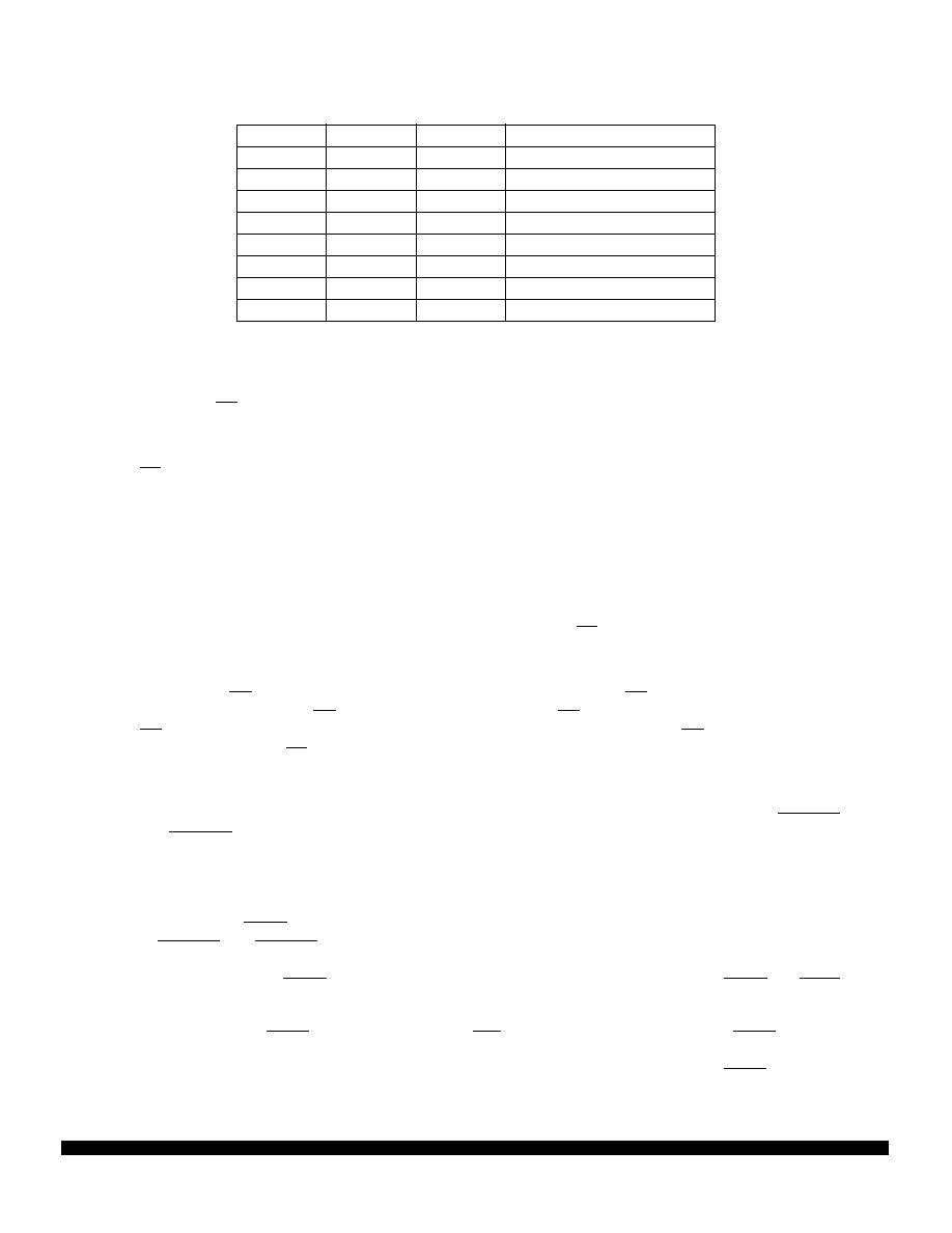
Table 9 CPU32 Address Space Encoding
FC2
FC1
FC0
Address Space
0
Reserved
0
1
User Data Space
0
1
0
User Program Space
0
1
Reserved
1
0
Reserved
1
0
1
Supervisor Data Space
1
0
Supervisor Program Space
1
CPU Space
相关PDF资料 |
PDF描述 |
|---|---|
| ML9203-XXGA | 16 X 35 DOTS FLUORESCENT DSPL CTRL, PQFP100 |
| M8813F2Y-15T1T | 128K X 8 FLASH, 27 I/O, PIA-GENERAL PURPOSE, PQFP52 |
| M34514M6-XXXFP | 4-BIT, MROM, 4.2 MHz, MICROCONTROLLER, PDSO42 |
| MC68376BGMFT20 | 32-BIT, MROM, 20.97 MHz, MICROCONTROLLER, PQFP16 |
| MC68HC11C0MFN2 | 8-BIT, 2 MHz, MICROCONTROLLER, PQCC68 |
相关代理商/技术参数 |
参数描述 |
|---|---|
| MC68LK332GCPV16 | 功能描述:IC MCU 32BIT LV GMASK 144-LQFP RoHS:否 类别:集成电路 (IC) >> 嵌入式 - 微控制器, 系列:M683xx 其它有关文件:STM32F101T8 View All Specifications 特色产品:STM32 32-bit Cortex MCUs 标准包装:490 系列:STM32 F1 核心处理器:ARM? Cortex?-M3 芯体尺寸:32-位 速度:36MHz 连通性:I²C,IrDA,LIN,SPI,UART/USART 外围设备:DMA,PDR,POR,PVD,PWM,温度传感器,WDT 输入/输出数:26 程序存储器容量:64KB(64K x 8) 程序存储器类型:闪存 EEPROM 大小:- RAM 容量:10K x 8 电压 - 电源 (Vcc/Vdd):2 V ~ 3.6 V 数据转换器:A/D 10x12b 振荡器型:内部 工作温度:-40°C ~ 85°C 封装/外壳:36-VFQFN,36-VFQFPN 包装:托盘 配用:497-10030-ND - STARTER KIT FOR STM32497-8853-ND - BOARD DEMO STM32 UNIV USB-UUSCIKSDKSTM32-PL-ND - KIT IAR KICKSTART STM32 CORTEXM3497-8512-ND - KIT STARTER FOR STM32F10XE MCU497-8505-ND - KIT STARTER FOR STM32F10XE MCU497-8304-ND - KIT STM32 MOTOR DRIVER BLDC497-6438-ND - BOARD EVALUTION FOR STM32 512K497-6289-ND - KIT PERFORMANCE STICK FOR STM32MCBSTM32UME-ND - BOARD EVAL MCBSTM32 + ULINK-MEMCBSTM32U-ND - BOARD EVAL MCBSTM32 + ULINK2更多... 其它名称:497-9032STM32F101T8U6-ND |
| MC68M360VR25VLR2 | 功能描述:微处理器 - MPU QUICC 2SMC 1SPI RoHS:否 制造商:Atmel 处理器系列:SAMA5D31 核心:ARM Cortex A5 数据总线宽度:32 bit 最大时钟频率:536 MHz 程序存储器大小:32 KB 数据 RAM 大小:128 KB 接口类型:CAN, Ethernet, LIN, SPI,TWI, UART, USB 工作电源电压:1.8 V to 3.3 V 最大工作温度:+ 85 C 安装风格:SMD/SMT 封装 / 箱体:FBGA-324 |
| MC68M360ZP25VLR2 | 功能描述:IC MPU QUICC 25MHZ 357-PBGA RoHS:否 类别:集成电路 (IC) >> 嵌入式 - 微处理器 系列:M683xx 标准包装:1 系列:MPC85xx 处理器类型:32-位 MPC85xx PowerQUICC III 特点:- 速度:1.2GHz 电压:1.1V 安装类型:表面贴装 封装/外壳:783-BBGA,FCBGA 供应商设备封装:783-FCPBGA(29x29) 包装:托盘 |
| MC68M360ZQ25VLR2 | 功能描述:微处理器 - MPU QUICC 2SMC 1SPI RoHS:否 制造商:Atmel 处理器系列:SAMA5D31 核心:ARM Cortex A5 数据总线宽度:32 bit 最大时钟频率:536 MHz 程序存储器大小:32 KB 数据 RAM 大小:128 KB 接口类型:CAN, Ethernet, LIN, SPI,TWI, UART, USB 工作电源电压:1.8 V to 3.3 V 最大工作温度:+ 85 C 安装风格:SMD/SMT 封装 / 箱体:FBGA-324 |
| MC68MH360AI25L | 功能描述:微处理器 - MPU QUICC 2SMC 1SPI RoHS:否 制造商:Atmel 处理器系列:SAMA5D31 核心:ARM Cortex A5 数据总线宽度:32 bit 最大时钟频率:536 MHz 程序存储器大小:32 KB 数据 RAM 大小:128 KB 接口类型:CAN, Ethernet, LIN, SPI,TWI, UART, USB 工作电源电压:1.8 V to 3.3 V 最大工作温度:+ 85 C 安装风格:SMD/SMT 封装 / 箱体:FBGA-324 |
发布紧急采购,3分钟左右您将得到回复。