- 您现在的位置:买卖IC网 > PDF目录80570 > MC68LK332GCFC16 (MOTOROLA INC) 32-BIT, 16.78 MHz, MICROCONTROLLER, PQFP132 PDF资料下载
参数资料
| 型号: | MC68LK332GCFC16 |
| 厂商: | MOTOROLA INC |
| 元件分类: | 微控制器/微处理器 |
| 英文描述: | 32-BIT, 16.78 MHz, MICROCONTROLLER, PQFP132 |
| 封装: | PLASTIC, QFP-132 |
| 文件页数: | 33/111页 |
| 文件大小: | 650K |
| 代理商: | MC68LK332GCFC16 |
第1页第2页第3页第4页第5页第6页第7页第8页第9页第10页第11页第12页第13页第14页第15页第16页第17页第18页第19页第20页第21页第22页第23页第24页第25页第26页第27页第28页第29页第30页第31页第32页当前第33页第34页第35页第36页第37页第38页第39页第40页第41页第42页第43页第44页第45页第46页第47页第48页第49页第50页第51页第52页第53页第54页第55页第56页第57页第58页第59页第60页第61页第62页第63页第64页第65页第66页第67页第68页第69页第70页第71页第72页第73页第74页第75页第76页第77页第78页第79页第80页第81页第82页第83页第84页第85页第86页第87页第88页第89页第90页第91页第92页第93页第94页第95页第96页第97页第98页第99页第100页第101页第102页第103页第104页第105页第106页第107页第108页第109页第110页第111页
MOTOROLA
MC68332
28
MC68332TS/D
3.4.8 Data Transfer Mechanism
The MCU architecture supports byte, word, and long-word operands, allowing access to 8- and 16-bit
data ports through the use of asynchronous cycles controlled by the data transfer and size acknowledge
inputs (DSACK1 and DSACK0).
3.4.9 Dynamic Bus Sizing
The MCU dynamically interprets the port size of the addressed device during each bus cycle, allowing
operand transfers to or from 8- and 16-bit ports. During an operand transfer cycle, the slave device sig-
nals its port size and indicates completion of the bus cycle to the MCU through the use of the DSACK0
and DSACK1 inputs, as shown in the following table.
For example, if the MCU is executing an instruction that reads a long-word operand from a 16-bit port,
the MCU latches the 16 bits of valid data and then runs another bus cycle to obtain the other 16 bits.
The operation for an 8-bit port is similar, but requires four read cycles. The addressed device uses the
DSACK0 and DSACK1 signals to indicate the port width. For instance, a 16-bit device always returns
DSACK0 = 1 and DSACK1 = 0 for a 16-bit port, regardless of whether the bus cycle is a byte or word
operation.
Dynamic bus sizing requires that the portion of the data bus used for a transfer to or from a particular
port size be fixed. A 16-bit port must reside on data bus bits [15:0] and an 8-bit port must reside on data
bus bits [15:8]. This minimizes the number of bus cycles needed to transfer data and ensures that the
MCU transfers valid data.
The MCU always attempts to transfer the maximum amount of data on all bus cycles. For a word oper-
ation, it is assumed that the port is 16 bits wide when the bus cycle begins. Operand bytes are desig-
nated as shown in the following figure. OP0 is the most significant byte of a long-word operand, and
OP3 is the least significant byte. The two bytes of a word-length operand are OP0 (most significant) and
OP1. The single byte of a byte-length operand is OP0.
Figure 8 Operand Byte Order
3.4.10 Operand Alignment
The data multiplexer establishes the necessary connections for different combinations of address and
data sizes. The multiplexer takes the two bytes of the 16-bit bus and routes them to their required po-
sitions. Positioning of bytes is determined by the size and address outputs. SIZ1 and SIZ0 indicate the
remaining number of bytes to be transferred during the current bus cycle. The number of bytes trans-
ferred is equal to or less than the size indicated by SIZ1 and SIZ0, depending on port width.
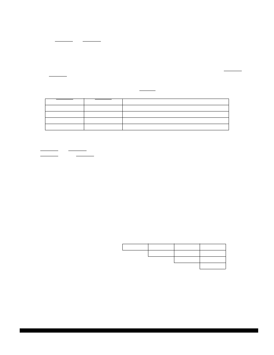
Table 10 Effect of DSACK Signals
DSACK1
DSACK0
Result
1
Insert Wait States in Current Bus Cycle
1
0
Complete Cycle —Data Bus Port Size is 8 Bits
0
1
Complete Cycle —Data Bus Port Size is 16 Bits
0
Reserved
Operand
Byte Order
31
24
23
16
15
8
7
0
Long Word
OP0
OP1
OP2
OP3
Three Byte
OP0
OP1
OP2
Word
OP0
OP1
Byte
OP0
相关PDF资料 |
PDF描述 |
|---|---|
| ML9203-XXGA | 16 X 35 DOTS FLUORESCENT DSPL CTRL, PQFP100 |
| M8813F2Y-15T1T | 128K X 8 FLASH, 27 I/O, PIA-GENERAL PURPOSE, PQFP52 |
| M34514M6-XXXFP | 4-BIT, MROM, 4.2 MHz, MICROCONTROLLER, PDSO42 |
| MC68376BGMFT20 | 32-BIT, MROM, 20.97 MHz, MICROCONTROLLER, PQFP16 |
| MC68HC11C0MFN2 | 8-BIT, 2 MHz, MICROCONTROLLER, PQCC68 |
相关代理商/技术参数 |
参数描述 |
|---|---|
| MC68LK332GCPV16 | 功能描述:IC MCU 32BIT LV GMASK 144-LQFP RoHS:否 类别:集成电路 (IC) >> 嵌入式 - 微控制器, 系列:M683xx 其它有关文件:STM32F101T8 View All Specifications 特色产品:STM32 32-bit Cortex MCUs 标准包装:490 系列:STM32 F1 核心处理器:ARM? Cortex?-M3 芯体尺寸:32-位 速度:36MHz 连通性:I²C,IrDA,LIN,SPI,UART/USART 外围设备:DMA,PDR,POR,PVD,PWM,温度传感器,WDT 输入/输出数:26 程序存储器容量:64KB(64K x 8) 程序存储器类型:闪存 EEPROM 大小:- RAM 容量:10K x 8 电压 - 电源 (Vcc/Vdd):2 V ~ 3.6 V 数据转换器:A/D 10x12b 振荡器型:内部 工作温度:-40°C ~ 85°C 封装/外壳:36-VFQFN,36-VFQFPN 包装:托盘 配用:497-10030-ND - STARTER KIT FOR STM32497-8853-ND - BOARD DEMO STM32 UNIV USB-UUSCIKSDKSTM32-PL-ND - KIT IAR KICKSTART STM32 CORTEXM3497-8512-ND - KIT STARTER FOR STM32F10XE MCU497-8505-ND - KIT STARTER FOR STM32F10XE MCU497-8304-ND - KIT STM32 MOTOR DRIVER BLDC497-6438-ND - BOARD EVALUTION FOR STM32 512K497-6289-ND - KIT PERFORMANCE STICK FOR STM32MCBSTM32UME-ND - BOARD EVAL MCBSTM32 + ULINK-MEMCBSTM32U-ND - BOARD EVAL MCBSTM32 + ULINK2更多... 其它名称:497-9032STM32F101T8U6-ND |
| MC68M360VR25VLR2 | 功能描述:微处理器 - MPU QUICC 2SMC 1SPI RoHS:否 制造商:Atmel 处理器系列:SAMA5D31 核心:ARM Cortex A5 数据总线宽度:32 bit 最大时钟频率:536 MHz 程序存储器大小:32 KB 数据 RAM 大小:128 KB 接口类型:CAN, Ethernet, LIN, SPI,TWI, UART, USB 工作电源电压:1.8 V to 3.3 V 最大工作温度:+ 85 C 安装风格:SMD/SMT 封装 / 箱体:FBGA-324 |
| MC68M360ZP25VLR2 | 功能描述:IC MPU QUICC 25MHZ 357-PBGA RoHS:否 类别:集成电路 (IC) >> 嵌入式 - 微处理器 系列:M683xx 标准包装:1 系列:MPC85xx 处理器类型:32-位 MPC85xx PowerQUICC III 特点:- 速度:1.2GHz 电压:1.1V 安装类型:表面贴装 封装/外壳:783-BBGA,FCBGA 供应商设备封装:783-FCPBGA(29x29) 包装:托盘 |
| MC68M360ZQ25VLR2 | 功能描述:微处理器 - MPU QUICC 2SMC 1SPI RoHS:否 制造商:Atmel 处理器系列:SAMA5D31 核心:ARM Cortex A5 数据总线宽度:32 bit 最大时钟频率:536 MHz 程序存储器大小:32 KB 数据 RAM 大小:128 KB 接口类型:CAN, Ethernet, LIN, SPI,TWI, UART, USB 工作电源电压:1.8 V to 3.3 V 最大工作温度:+ 85 C 安装风格:SMD/SMT 封装 / 箱体:FBGA-324 |
| MC68MH360AI25L | 功能描述:微处理器 - MPU QUICC 2SMC 1SPI RoHS:否 制造商:Atmel 处理器系列:SAMA5D31 核心:ARM Cortex A5 数据总线宽度:32 bit 最大时钟频率:536 MHz 程序存储器大小:32 KB 数据 RAM 大小:128 KB 接口类型:CAN, Ethernet, LIN, SPI,TWI, UART, USB 工作电源电压:1.8 V to 3.3 V 最大工作温度:+ 85 C 安装风格:SMD/SMT 封装 / 箱体:FBGA-324 |
发布紧急采购,3分钟左右您将得到回复。