- 您现在的位置:买卖IC网 > PDF目录45250 > MC7457VG1000LC (FREESCALE SEMICONDUCTOR INC) 32-BIT, 1000 MHz, RISC PROCESSOR, CBGA483 PDF资料下载
参数资料
| 型号: | MC7457VG1000LC |
| 厂商: | FREESCALE SEMICONDUCTOR INC |
| 元件分类: | 微控制器/微处理器 |
| 英文描述: | 32-BIT, 1000 MHz, RISC PROCESSOR, CBGA483 |
| 封装: | 29 X 29 MM, 3.22 MM HEIGHT, 1.27 MM PITCH, ROHS COMPLIANT, CERAMIC, BGA-483 |
| 文件页数: | 14/73页 |
| 文件大小: | 1715K |
| 代理商: | MC7457VG1000LC |
第1页第2页第3页第4页第5页第6页第7页第8页第9页第10页第11页第12页第13页当前第14页第15页第16页第17页第18页第19页第20页第21页第22页第23页第24页第25页第26页第27页第28页第29页第30页第31页第32页第33页第34页第35页第36页第37页第38页第39页第40页第41页第42页第43页第44页第45页第46页第47页第48页第49页第50页第51页第52页第53页第54页第55页第56页第57页第58页第59页第60页第61页第62页第63页第64页第65页第66页第67页第68页第69页第70页第71页第72页第73页
MPC7457 RISC Microprocessor Hardware Specifications, Rev. 7
Freescale Semiconductor
21
Electrical and Thermal Characteristics
5.2.3
L3 Clock AC Specifications
The L3_CLK frequency is programmed by the L3 configuration register core-to-L3 divisor ratio. See
Table 18 for example core and L3 frequencies at various divisors. Table 10 provides the potential range of
L3_CLK output AC timing specifications as defined in Figure 7.
The maximum L3_CLK frequency is the core frequency divided by two. Given the high core frequencies
available in the MPC7457, however, most SRAM designs will be not be able to operate in this mode using
current technology and, as a result, will select a greater core-to-L3 divisor to provide a longer L3_CLK
period for read and write access to the L3 SRAMs. Therefore, the typical L3_CLK frequency shown in
Table 10 is considered to be the practical maximum in a typical system. The maximum L3_CLK frequency
for any application of the MPC7457 will be a function of the AC timings of the MPC7457, the AC timings
for the SRAM, bus loading, and printed-circuit board trace length, and may be greater or less than the value
given in Table 10. Note that SYSCLK input jitter and L3_CLK[0:1] output jitter are already
comprehended in the L3 bus AC timing specifications and do not need to be separately accounted for in
an L3 AC timing analysis. Clock skews, where applicable, do need to be accounted for in an AC timing
analysis.
Freescale is similarly limited by system constraints and cannot perform tests of the L3 interface on a
socketed part on a functional tester at the maximum frequencies of Table 10. Therefore, functional
operation and AC timing information are tested at core-to-L3 divisors which result in L3 frequencies at
250 MHz or lower.
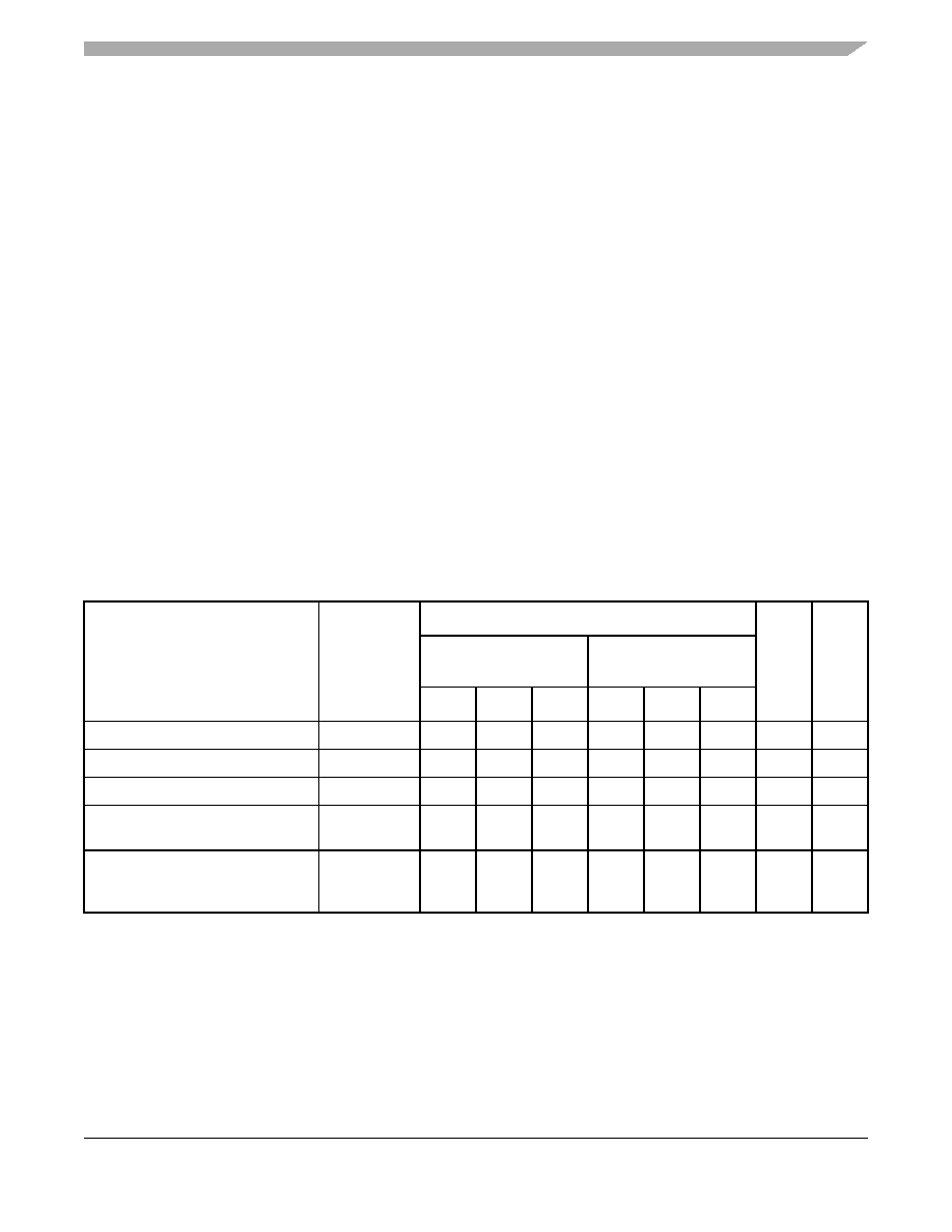
Table 10. L3_CLK Output AC Timing Specifications
At recommended operating conditions. See Table 4.
Parameter
Symbol
Device Revision (L3 I/O Voltage) 6
Unit
Notes
Rev 1.1. (All I/O Modes)
Rev 1.2 (1.5-V I/O Mode)
Rev 1.2
(1.8-, 2.5-V I/O Modes)
Min
Typ
Max
Min
Typ
Max
L3 clock frequency
fL3_CLK
—200
—
250—
MHz
1
L3 clock cycle time
tL3_CLK
—
5.0
—
4.0
—
ns
1
L3 clock duty cycle
tCHCL/tL3_CLK
—50—
%
2
L3 clock output-to-output skew
(L3_CLK0 to L3_CLK1)
tL3CSKW1
—
100
—
100
ps
3
L3 clock output-to-output skew
(L3_CLK[0:1] to
L3_ECHO_CLK[1,3])
tL3CSKW2
—
100
—
100
ps
4
相关PDF资料 |
PDF描述 |
|---|---|
| MC7457RX867NC | 32-BIT, 867 MHz, RISC PROCESSOR, CBGA483 |
| MC7457VG867NC | 32-BIT, 867 MHz, RISC PROCESSOR, CBGA483 |
| MC7457RX1267LC | 32-BIT, 1267 MHz, RISC PROCESSOR, CBGA483 |
| MC7457VG733NC | 32-BIT, 733 MHz, RISC PROCESSOR, CBGA483 |
| MC74ACT125DR2 | ACT SERIES, QUAD 1-BIT DRIVER, TRUE OUTPUT, PDSO14 |
相关代理商/技术参数 |
参数描述 |
|---|---|
| MC7457VG1000NC | 功能描述:微处理器 - MPU APOLO7 RV1.2 1.1V 105C RoHS:否 制造商:Atmel 处理器系列:SAMA5D31 核心:ARM Cortex A5 数据总线宽度:32 bit 最大时钟频率:536 MHz 程序存储器大小:32 KB 数据 RAM 大小:128 KB 接口类型:CAN, Ethernet, LIN, SPI,TWI, UART, USB 工作电源电压:1.8 V to 3.3 V 最大工作温度:+ 85 C 安装风格:SMD/SMT 封装 / 箱体:FBGA-324 |
| MC7457VG1267LC | 功能描述:微处理器 - MPU APOLO7 RV1.2 1.3V 105C RoHS:否 制造商:Atmel 处理器系列:SAMA5D31 核心:ARM Cortex A5 数据总线宽度:32 bit 最大时钟频率:536 MHz 程序存储器大小:32 KB 数据 RAM 大小:128 KB 接口类型:CAN, Ethernet, LIN, SPI,TWI, UART, USB 工作电源电压:1.8 V to 3.3 V 最大工作温度:+ 85 C 安装风格:SMD/SMT 封装 / 箱体:FBGA-324 |
| MC7457VG733NC | 功能描述:IC MPU RISC 733MHZ 483FCCBGA RoHS:是 类别:集成电路 (IC) >> 嵌入式 - 微处理器 系列:MPC74xx 标准包装:1 系列:MPC85xx 处理器类型:32-位 MPC85xx PowerQUICC III 特点:- 速度:1.2GHz 电压:1.1V 安装类型:表面贴装 封装/外壳:783-BBGA,FCBGA 供应商设备封装:783-FCPBGA(29x29) 包装:托盘 |
| MC7457VG867NC | 功能描述:微处理器 - MPU APOLO7 RV1.2 1.1V 105C RoHS:否 制造商:Atmel 处理器系列:SAMA5D31 核心:ARM Cortex A5 数据总线宽度:32 bit 最大时钟频率:536 MHz 程序存储器大小:32 KB 数据 RAM 大小:128 KB 接口类型:CAN, Ethernet, LIN, SPI,TWI, UART, USB 工作电源电压:1.8 V to 3.3 V 最大工作温度:+ 85 C 安装风格:SMD/SMT 封装 / 箱体:FBGA-324 |
| MC74A5-33SNTR | 制造商:Rochester Electronics LLC 功能描述:- Tape and Reel |
发布紧急采购,3分钟左右您将得到回复。