- 您现在的位置:买卖IC网 > PDF目录26800 > MC74AC00M (ON SEMICONDUCTOR) AC SERIES, QUAD 2-INPUT NAND GATE, PDSO14 PDF资料下载
参数资料
| 型号: | MC74AC00M |
| 厂商: | ON SEMICONDUCTOR |
| 元件分类: | 门电路 |
| 英文描述: | AC SERIES, QUAD 2-INPUT NAND GATE, PDSO14 |
| 封装: | EIAJ, PLASTIC, 14 PIN |
| 文件页数: | 11/45页 |
| 文件大小: | 434K |
| 代理商: | MC74AC00M |
第1页第2页第3页第4页第5页第6页第7页第8页第9页第10页当前第11页第12页第13页第14页第15页第16页第17页第18页第19页第20页第21页第22页第23页第24页第25页第26页第27页第28页第29页第30页第31页第32页第33页第34页第35页第36页第37页第38页第39页第40页第41页第42页第43页第44页第45页
http://onsemi.com
23
DC CHARACTERISTICS for ‘ACT Family Devices (continued)
Symbol
Conditions
Unit
74ACT
VCC
(V)
Parameter
Symbol
Conditions
Unit
TA =
–40
°C to +85°C
TA = 25°C
VCC
(V)
Parameter
Symbol
Conditions
Unit
Guaranteed Limits
Typ
VCC
(V)
Parameter
4.5
0.36
0.44
V
IOL
24 mA
5.5
0.36
0.44
IOL
24 mA
IIN
Maximum Input
55
±01
±10
A
VI =VCC GND
Leakage Current
5.5
±0.1
±1.0
A
VI = VCC, GND
ICCT
Additional Max. ICC/Input
5.5
0.6
1.5
mA
VI = VCC – 2.1V
IOLD
Minimum Dynamic
Ot
t C
t
5.5
75
mA
VOLD = 1.65 V Max
IOHD
Output Current
5.5
–75
mA
VOHD = 3.85 V Min
ICC
Maximum Quiescent
55
80
A
VIN =VCC or GND
Q
Supply Current
5.5
8.0
80
A
VIN = VCC or GND
* All outputs loaded; thresholds on input associated with output under test.
Maximum test duration 2.0 ms, one output loaded at a time.
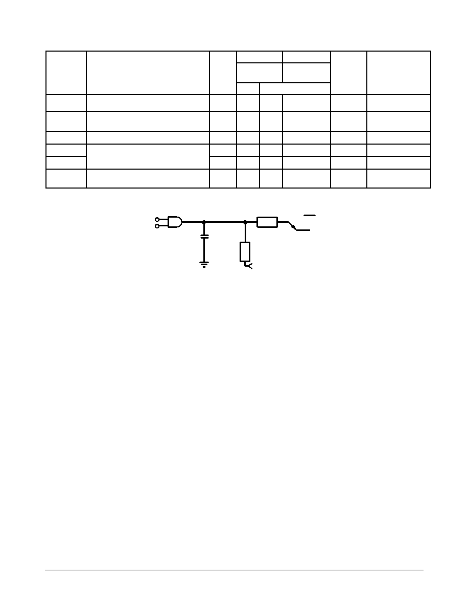
TEST LOAD
50 pF
tr = 3 ns
tf = 3 ns
OPEN
2 × VCC
500
450
50 SCOPE
DUT
Figure 1–21. AC Tri-State Loading Circuit
tPZH
tPHZ
tPZL
tPLZ
AC Loading and Waveforms
Loading Circuit
Figure 1–21 shows the AC loading circuit used in
characterizing and specifying propagation delays of all
FACT devices (‘AC and ‘ACT) unless otherwise specified
in the data sheet of a specific device.
The use of this load, differs somewhat from previous
(HCMOS) practice, provides more meaningful information
and minimizes problems of instrumentation and customer
correlation. In the past, +25
°C propagation delays for TTL
devices were specified with a load of 15 pF to ground; this
required great care in building test jigs to minimize stray
capacitance and implied the use of high impedance, high
frequency scope probes. FAST circuits changed to 50 pF of
capacitance allowing more leeway in stray capacitance and
also loading the device during rising or falling output
transitions. This more closely resembles the inloading to be
expected in average applications and thus gives the designer
more useful delay figures. We have incorporated this
scheme into the FACT product line. The net effect of the
change in AC load is to increase the average observed
propagation delay by about 1 ns.
The 500 ohm resistor to ground can be a high frequency
passive probe for a sampling oscilloscope, which costs much
less than the equivalent high impedance probe. Alternately,
the 500 ohm resistor to ground can simply be a 450 ohm
resistor feeding into a 50 ohm coaxial cable leading to a
sampling scope input connector, with the internal 50 ohm
termination of the scope completing the path to ground. This
is the preferred scheme for correlation. (See Figure 1–21.)
With this scheme there should be a matching cable from the
device input pin to the other input of the sampling scope; this
also serves as a 50 ohm termination for the pulse generator
that supplies the input signal.
Shown in Figure 1–21 is a second 500 ohm resistor from
the device output to a switch. For most measurements this
switch is open; it is closed for measuring one set of the
Enable/Disable
parameters
(LOW-to-OFF
and
OFF-to-LOW) of a 3-state output. With the switch closed,
the pair of 500 ohm resistors and the 2
× VCC supply voltage
establish a quiescent HIGH level.
相关PDF资料 |
PDF描述 |
|---|---|
| MC74AC04MR1 | AC SERIES, HEX 1-INPUT INVERT GATE, PDSO14 |
| MC74AC05MR2 | AC SERIES, HEX 1-INPUT INVERT GATE, PDSO14 |
| MC74ACT05DT | ACT SERIES, HEX 1-INPUT INVERT GATE, PDSO14 |
| MC74AC109N | AC SERIES, DUAL POSITIVE EDGE TRIGGERED J-KBAR FLIP-FLOP, COMPLEMENTARY OUTPUT, PDIP16 |
| MC74AC109D | AC SERIES, DUAL POSITIVE EDGE TRIGGERED J-KBAR FLIP-FLOP, COMPLEMENTARY OUTPUT, PDSO16 |
相关代理商/技术参数 |
参数描述 |
|---|---|
| MC74AC00MEL | 功能描述:逻辑门 2-6V Quad 2-Input RoHS:否 制造商:Texas Instruments 产品:OR 逻辑系列:LVC 栅极数量:2 线路数量(输入/输出):2 / 1 高电平输出电流:- 16 mA 低电平输出电流:16 mA 传播延迟时间:3.8 ns 电源电压-最大:5.5 V 电源电压-最小:1.65 V 最大工作温度:+ 125 C 安装风格:SMD/SMT 封装 / 箱体:DCU-8 封装:Reel |
| MC74AC00MELG | 功能描述:逻辑门 2-6V Quad 2-Input NAND RoHS:否 制造商:Texas Instruments 产品:OR 逻辑系列:LVC 栅极数量:2 线路数量(输入/输出):2 / 1 高电平输出电流:- 16 mA 低电平输出电流:16 mA 传播延迟时间:3.8 ns 电源电压-最大:5.5 V 电源电压-最小:1.65 V 最大工作温度:+ 125 C 安装风格:SMD/SMT 封装 / 箱体:DCU-8 封装:Reel |
| MC74AC00ML1 | 制造商:Rochester Electronics LLC 功能描述:- Bulk |
| MC74AC00MR1 | 制造商:Rochester Electronics LLC 功能描述:- Bulk |
| MC74AC00N | 功能描述:逻辑门 2-6V Quad 2-Input RoHS:否 制造商:Texas Instruments 产品:OR 逻辑系列:LVC 栅极数量:2 线路数量(输入/输出):2 / 1 高电平输出电流:- 16 mA 低电平输出电流:16 mA 传播延迟时间:3.8 ns 电源电压-最大:5.5 V 电源电压-最小:1.65 V 最大工作温度:+ 125 C 安装风格:SMD/SMT 封装 / 箱体:DCU-8 封装:Reel |
发布紧急采购,3分钟左右您将得到回复。