- 您现在的位置:买卖IC网 > PDF目录26800 > MC74AC00M (ON SEMICONDUCTOR) AC SERIES, QUAD 2-INPUT NAND GATE, PDSO14 PDF资料下载
参数资料
| 型号: | MC74AC00M |
| 厂商: | ON SEMICONDUCTOR |
| 元件分类: | 门电路 |
| 英文描述: | AC SERIES, QUAD 2-INPUT NAND GATE, PDSO14 |
| 封装: | EIAJ, PLASTIC, 14 PIN |
| 文件页数: | 3/45页 |
| 文件大小: | 434K |
| 代理商: | MC74AC00M |
第1页第2页当前第3页第4页第5页第6页第7页第8页第9页第10页第11页第12页第13页第14页第15页第16页第17页第18页第19页第20页第21页第22页第23页第24页第25页第26页第27页第28页第29页第30页第31页第32页第33页第34页第35页第36页第37页第38页第39页第40页第41页第42页第43页第44页第45页
http://onsemi.com
15
Section 2 – Circuit Characteristics
Power Dissipation
One advantage to using CMOS logic is its extremely low
power consumption. During quiescent conditions, FACT
will consume several orders of magnitude less current than
its bipolar counterparts. But DC power consumption is not
the whole picture. Any circuit will have AC power
consumption, whether it is built with CMOS or bipolar
technologies.
Power consumption of a circuit can be calculated using
the formula:
PD = [(CL + CPD) VCC VS f] + [IQ VCC]
where
PD
= power dissipation (W)
CL
= load capacitance (Farad)
CPD
= device power capacitance (Farad)
VCC
= power supply (Volt)
VS
= output voltage swing (Volt)
f
= frequency of operation (Hz)
IQ
= quiescent current (Amp)
Power consumption for FACT is dependent on the supply
voltage, frequency of operation, internal capacitance and
load. VS will be VCC and IQ can be considered negligible for
CMOS. Therefore, the simplified formula for CMOS is:
PD = (CL + CPD) VCC2 f
CPD values for CMOS devices are calculated by
measuring the power consumption of a device at two
different frequencies. CPD is calculated in the following
manner:
1. The power supply voltage is set to VCC = 5 Vdc.
2. Signal inputs are set up so that as many outputs as
possible are switching, giving a worst-case situation
per JEDEC CPD conditions (see Section 3).
3. The power supply current is measured and recorded
at input frequencies of 200 kHz and 1 MHz.
4. The power dissipation capacitance is calculated by
solving the two simultaneous equations
P1 = (CPD VCC2 f1) + (ICC VCC)
P2 = (CPD VCC2 f2) + (ICC VCC)
giving
CPD = (P1 – P2)/VCC2(f1 – f2)
or
CPD = (I1 – I2)/VCC(f1 – f2)
where
I1 = supply current at f1 = 200 kHz.
I2 = supply current at f2 = 1 MHz.
On FACT device data sheets, CPD is a typical value and is
given either for the package or for the individual device
function, if there is more than one (i.e., gates, flip-flops,
etc.), within the package.
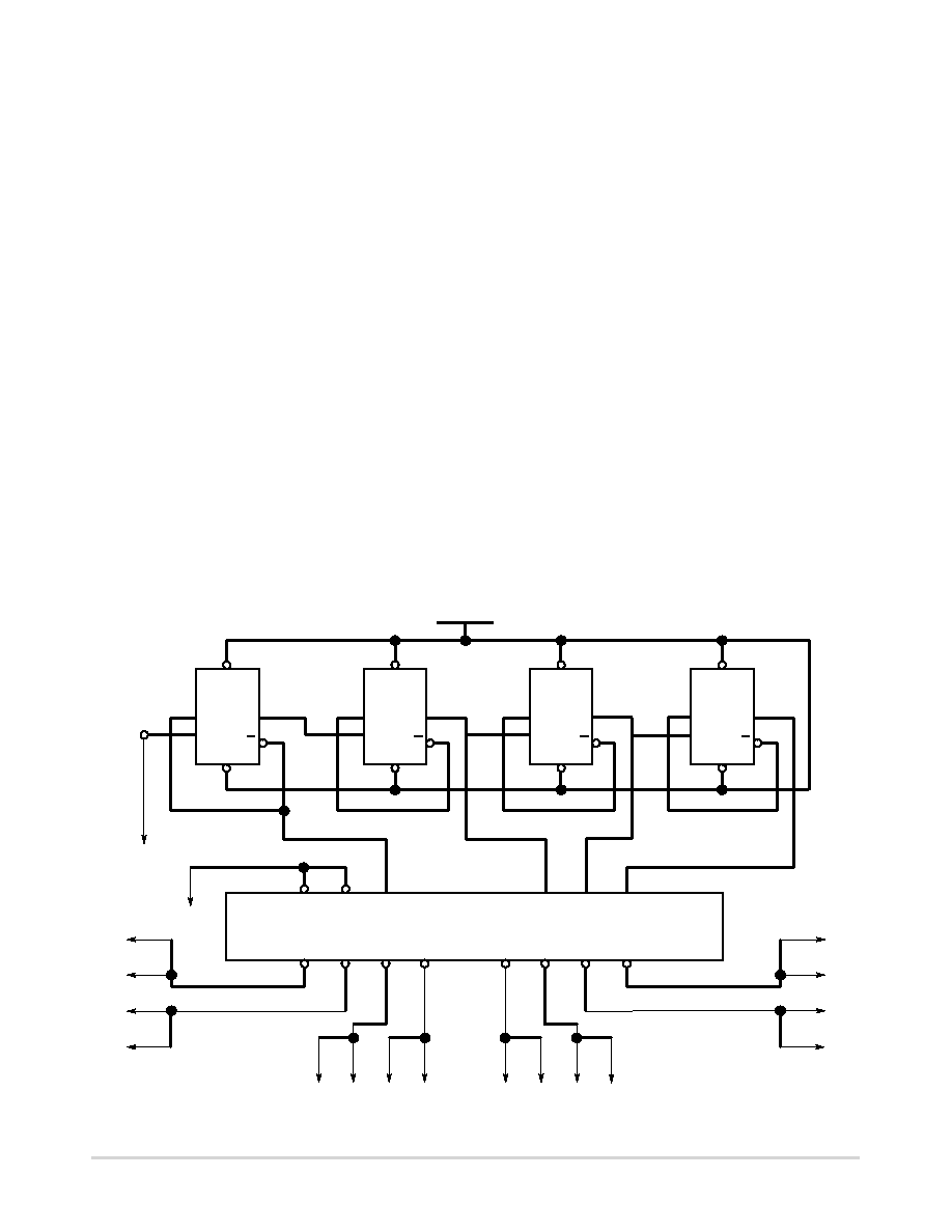
SET
Q
CLK
D
MC74AC74
CLR
SET
Q
CLK
D
MC74AC74
CLR
SET
Q
CLK
D
MC74AC74
CLR
SET
Q
CLK
D
MC74AC74
E1
E2
E3
A0
A1
A2
O1
O2
O3
O4
O5
O6
O7O8
INPUT
MC74AC04 LOAD DEVICES
MC74AC138
VCC
CLR
Figure 1–9. Power Demonstration Circuit Schematic
相关PDF资料 |
PDF描述 |
|---|---|
| MC74AC04MR1 | AC SERIES, HEX 1-INPUT INVERT GATE, PDSO14 |
| MC74AC05MR2 | AC SERIES, HEX 1-INPUT INVERT GATE, PDSO14 |
| MC74ACT05DT | ACT SERIES, HEX 1-INPUT INVERT GATE, PDSO14 |
| MC74AC109N | AC SERIES, DUAL POSITIVE EDGE TRIGGERED J-KBAR FLIP-FLOP, COMPLEMENTARY OUTPUT, PDIP16 |
| MC74AC109D | AC SERIES, DUAL POSITIVE EDGE TRIGGERED J-KBAR FLIP-FLOP, COMPLEMENTARY OUTPUT, PDSO16 |
相关代理商/技术参数 |
参数描述 |
|---|---|
| MC74AC00MEL | 功能描述:逻辑门 2-6V Quad 2-Input RoHS:否 制造商:Texas Instruments 产品:OR 逻辑系列:LVC 栅极数量:2 线路数量(输入/输出):2 / 1 高电平输出电流:- 16 mA 低电平输出电流:16 mA 传播延迟时间:3.8 ns 电源电压-最大:5.5 V 电源电压-最小:1.65 V 最大工作温度:+ 125 C 安装风格:SMD/SMT 封装 / 箱体:DCU-8 封装:Reel |
| MC74AC00MELG | 功能描述:逻辑门 2-6V Quad 2-Input NAND RoHS:否 制造商:Texas Instruments 产品:OR 逻辑系列:LVC 栅极数量:2 线路数量(输入/输出):2 / 1 高电平输出电流:- 16 mA 低电平输出电流:16 mA 传播延迟时间:3.8 ns 电源电压-最大:5.5 V 电源电压-最小:1.65 V 最大工作温度:+ 125 C 安装风格:SMD/SMT 封装 / 箱体:DCU-8 封装:Reel |
| MC74AC00ML1 | 制造商:Rochester Electronics LLC 功能描述:- Bulk |
| MC74AC00MR1 | 制造商:Rochester Electronics LLC 功能描述:- Bulk |
| MC74AC00N | 功能描述:逻辑门 2-6V Quad 2-Input RoHS:否 制造商:Texas Instruments 产品:OR 逻辑系列:LVC 栅极数量:2 线路数量(输入/输出):2 / 1 高电平输出电流:- 16 mA 低电平输出电流:16 mA 传播延迟时间:3.8 ns 电源电压-最大:5.5 V 电源电压-最小:1.65 V 最大工作温度:+ 125 C 安装风格:SMD/SMT 封装 / 箱体:DCU-8 封装:Reel |
发布紧急采购,3分钟左右您将得到回复。