- 您现在的位置:买卖IC网 > PDF目录3791 > MC908QC8CDRE (Freescale Semiconductor)IC MCU 8BIT 8K FLASH 28-TSSOP PDF资料下载
参数资料
| 型号: | MC908QC8CDRE |
| 厂商: | Freescale Semiconductor |
| 文件页数: | 86/275页 |
| 文件大小: | 0K |
| 描述: | IC MCU 8BIT 8K FLASH 28-TSSOP |
| 标准包装: | 50 |
| 系列: | HC08 |
| 核心处理器: | HC08 |
| 芯体尺寸: | 8-位 |
| 速度: | 8MHz |
| 连通性: | SCI,SPI |
| 外围设备: | LVD,POR,PWM |
| 输入/输出数: | 24 |
| 程序存储器容量: | 8KB(8K x 8) |
| 程序存储器类型: | 闪存 |
| RAM 容量: | 384 x 8 |
| 电压 - 电源 (Vcc/Vdd): | 3 V ~ 5.5 V |
| 数据转换器: | A/D 10x10b |
| 振荡器型: | 内部 |
| 工作温度: | -40°C ~ 85°C |
| 封装/外壳: | 28-TSSOP(0.173",4.40mm 宽) |
| 包装: | 管件 |
| 产品目录页面: | 725 (CN2011-ZH PDF) |
第1页第2页第3页第4页第5页第6页第7页第8页第9页第10页第11页第12页第13页第14页第15页第16页第17页第18页第19页第20页第21页第22页第23页第24页第25页第26页第27页第28页第29页第30页第31页第32页第33页第34页第35页第36页第37页第38页第39页第40页第41页第42页第43页第44页第45页第46页第47页第48页第49页第50页第51页第52页第53页第54页第55页第56页第57页第58页第59页第60页第61页第62页第63页第64页第65页第66页第67页第68页第69页第70页第71页第72页第73页第74页第75页第76页第77页第78页第79页第80页第81页第82页第83页第84页第85页当前第86页第87页第88页第89页第90页第91页第92页第93页第94页第95页第96页第97页第98页第99页第100页第101页第102页第103页第104页第105页第106页第107页第108页第109页第110页第111页第112页第113页第114页第115页第116页第117页第118页第119页第120页第121页第122页第123页第124页第125页第126页第127页第128页第129页第130页第131页第132页第133页第134页第135页第136页第137页第138页第139页第140页第141页第142页第143页第144页第145页第146页第147页第148页第149页第150页第151页第152页第153页第154页第155页第156页第157页第158页第159页第160页第161页第162页第163页第164页第165页第166页第167页第168页第169页第170页第171页第172页第173页第174页第175页第176页第177页第178页第179页第180页第181页第182页第183页第184页第185页第186页第187页第188页第189页第190页第191页第192页第193页第194页第195页第196页第197页第198页第199页第200页第201页第202页第203页第204页第205页第206页第207页第208页第209页第210页第211页第212页第213页第214页第215页第216页第217页第218页第219页第220页第221页第222页第223页第224页第225页第226页第227页第228页第229页第230页第231页第232页第233页第234页第235页第236页第237页第238页第239页第240页第241页第242页第243页第244页第245页第246页第247页第248页第249页第250页第251页第252页第253页第254页第255页第256页第257页第258页第259页第260页第261页第262页第263页第264页第265页第266页第267页第268页第269页第270页第271页第272页第273页第274页第275页
Functional Description
MC68HC908QC16 MC68HC908QC8 MC68HC908QC4 Data Sheet, Rev. 5
Freescale Semiconductor
175
pin of the master must be high or must be reconfigured as general-purpose I/O not affecting the SPI. (See
15.3.6.2 Mode Fault Error.) When CPHA = 1, the master begins driving its MOSI pin on the first SPSCK
edge. Therefore, the slave uses the first SPSCK edge as a start transmission signal. The SS pin can
remain low between transmissions. This format may be preferable in systems having only one master and
only one slave driving the MISO data line.
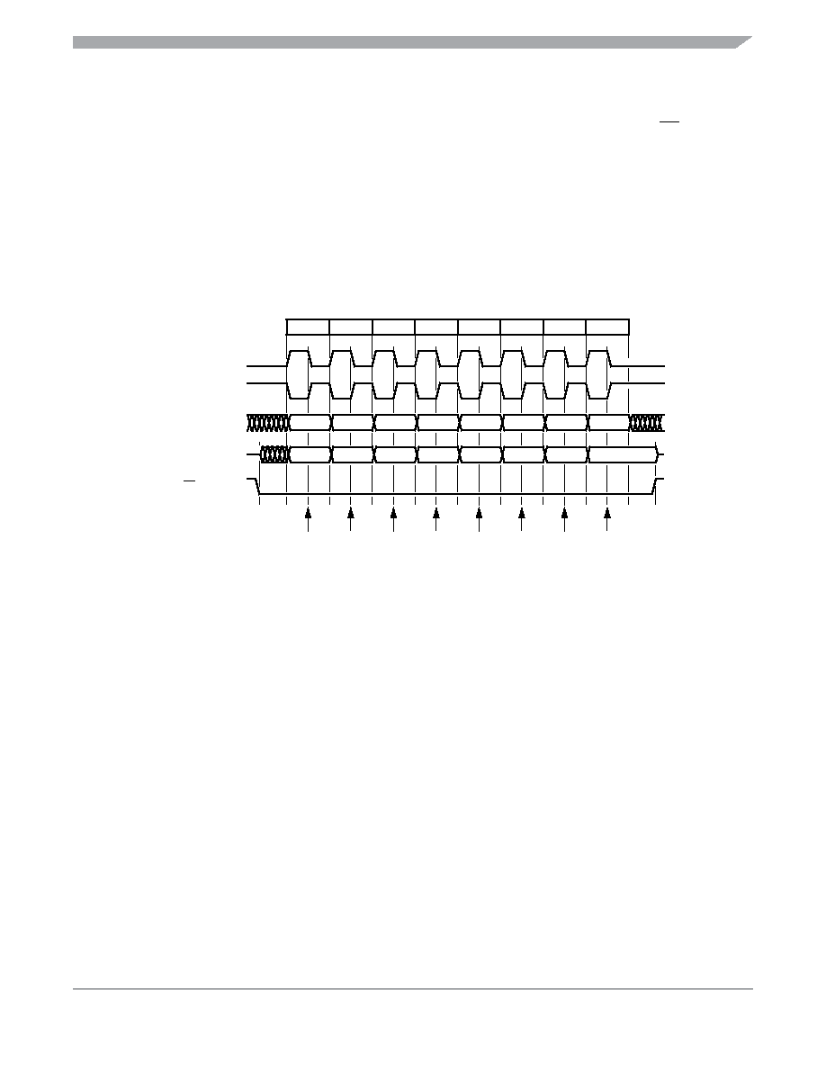
When CPHA = 1 for a slave, the first edge of the SPSCK indicates the beginning of the transmission. This
causes the SPI to leave its idle state and begin driving the MISO pin with the MSB of its data. After the
transmission begins, no new data is allowed into the shift register from the transmit data register.
Therefore, the SPI data register of the slave must be loaded with transmit data before the first edge of
SPSCK. Any data written after the first edge is stored in the transmit data register and transferred to the
shift register after the current transmission.
Figure 15-6. Transmission Format (CPHA = 1)
15.3.3.4 Transmission Initiation Latency
When the SPI is configured as a master (SPMSTR = 1), writing to the SPDR starts a transmission. CPHA
has no effect on the delay to the start of the transmission, but it does affect the initial state of the SPSCK
signal. When CPHA = 0, the SPSCK signal remains inactive for the first half of the first SPSCK cycle.
When CPHA = 1, the first SPSCK cycle begins with an edge on the SPSCK line from its inactive to its
active level. The SPI clock rate (selected by SPR1:SPR0) affects the delay from the write to SPDR and
the start of the SPI transmission. (See Figure 15-7.) The internal SPI clock in the master is a free-running
derivative of the internal MCU clock. To conserve power, it is enabled only when both the SPE and
SPMSTR bits are set. Because the SPI clock is free-running, it is uncertain where the write to the SPDR
occurs relative to the slower SPSCK. This uncertainty causes the variation in the initiation delay shown
in Figure 15-7. This delay is no longer than a single SPI bit time. That is, the maximum delay is two MCU
bus cycles for DIV2, eight MCU bus cycles for DIV8, 32 MCU bus cycles for DIV32, and 128 MCU bus
cycles for DIV128.
BIT 6
BIT 5
BIT 4
BIT 3
BIT 2
BIT 1
LSB
MSB
BIT 6
BIT 5
BIT 4
BIT 3
BIT 2
BIT 1
LSB
MSB
123
4
56
78
SPSCK CYCLE #
FOR REFERENCE
SPSCK; CPOL = 0
SPSCK; CPOL =1
MOSI
FROM MASTER
MISO
FROM SLAVE
SS; TO SLAVE
CAPTURE STROBE
相关PDF资料 |
PDF描述 |
|---|---|
| MC9S08SE4VWL | MCU 8BIT 4K FLASH 5V 28-SOIC |
| MC9S08SE4VTG | MCU 8BIT 4K FLASH 5V 16-TSSOP |
| MC9S08SE4VRL | MCU 8BIT 4K FLASH 5V 28-DIP |
| MC9S08SE4MTG | MCU 8BIT 4K FLASH 5V 16-TSSOP |
| MC9S08SE4MRL | MCU 8BIT 4K FLASH 5V 28-DIP |
相关代理商/技术参数 |
参数描述 |
|---|---|
| MC908QC8CDRER | 制造商:FREESCALE 制造商全称:Freescale Semiconductor, Inc 功能描述:Microcontrollers |
| MC908QC8CDSE | 功能描述:8位微控制器 -MCU 8BIT MCU 8KFLASH PB FREE RoHS:否 制造商:Silicon Labs 核心:8051 处理器系列:C8051F39x 数据总线宽度:8 bit 最大时钟频率:50 MHz 程序存储器大小:16 KB 数据 RAM 大小:1 KB 片上 ADC:Yes 工作电源电压:1.8 V to 3.6 V 工作温度范围:- 40 C to + 105 C 封装 / 箱体:QFN-20 安装风格:SMD/SMT |
| MC908QC8CDSER | 制造商:FREESCALE 制造商全称:Freescale Semiconductor, Inc 功能描述:Microcontrollers |
| MC908QC8CDTE | 功能描述:8位微控制器 -MCU 8BIT MCU 8KFLASH PB FREE RoHS:否 制造商:Silicon Labs 核心:8051 处理器系列:C8051F39x 数据总线宽度:8 bit 最大时钟频率:50 MHz 程序存储器大小:16 KB 数据 RAM 大小:1 KB 片上 ADC:Yes 工作电源电压:1.8 V to 3.6 V 工作温度范围:- 40 C to + 105 C 封装 / 箱体:QFN-20 安装风格:SMD/SMT |
| MC908QC8CDTER | 制造商:FREESCALE 制造商全称:Freescale Semiconductor, Inc 功能描述:Microcontrollers |
发布紧急采购,3分钟左右您将得到回复。