- 您现在的位置:买卖IC网 > PDF目录10943 > MC9328MX21SCVK (Freescale Semiconductor)IC MCU I.MX21 266MHZ 289-MAPBGA PDF资料下载
参数资料
| 型号: | MC9328MX21SCVK |
| 厂商: | Freescale Semiconductor |
| 文件页数: | 11/88页 |
| 文件大小: | 0K |
| 描述: | IC MCU I.MX21 266MHZ 289-MAPBGA |
| 标准包装: | 152 |
| 系列: | i.MX21 |
| 核心处理器: | ARM9 |
| 芯体尺寸: | 32-位 |
| 速度: | 266MHz |
| 连通性: | 1 线,EBI/EMI,I²C,IrDA,MMC,智能卡,SPI,SSI,UART/USART,USB OTG |
| 外围设备: | DMA,I²S,LCD,POR,PWM,WDT |
| 输入/输出数: | 192 |
| 程序存储器类型: | ROMless |
| 电压 - 电源 (Vcc/Vdd): | 1.45 V ~ 3.3 V |
| 振荡器型: | 外部 |
| 工作温度: | -40°C ~ 85°C |
| 封装/外壳: | 289-LFBGA |
| 包装: | 托盘 |
第1页第2页第3页第4页第5页第6页第7页第8页第9页第10页当前第11页第12页第13页第14页第15页第16页第17页第18页第19页第20页第21页第22页第23页第24页第25页第26页第27页第28页第29页第30页第31页第32页第33页第34页第35页第36页第37页第38页第39页第40页第41页第42页第43页第44页第45页第46页第47页第48页第49页第50页第51页第52页第53页第54页第55页第56页第57页第58页第59页第60页第61页第62页第63页第64页第65页第66页第67页第68页第69页第70页第71页第72页第73页第74页第75页第76页第77页第78页第79页第80页第81页第82页第83页第84页第85页第86页第87页第88页
Specifications
MC9328MX21S Technical Data, Rev. 1.3
Freescale Semiconductor
19
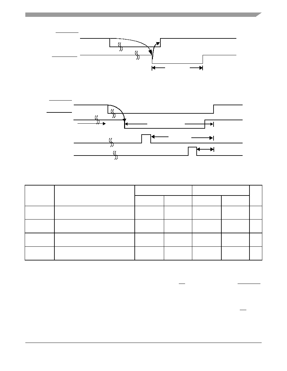
Figure 4. Assertion of DMA External Grant Signal
Figure 5 shows the safe maximum time for which External DMA request can be kept asserted, after
sensing grant signal active such that a new burst is not initiated.
Figure 5. Safe Maximum Timings for External Request De-Assertion
3.8
CSPI Timing Diagrams
To use the internal transmit (TX) and receive (RX) data FIFOs when the CSPI1 module is configured as a
master, two control signals are used for data transfer rate control: the SS signal (output) and the SPI_RDY
signal (input). The SPI 1 Sample Period Control Register (PERIODREG1) and the SPI 2 Sample Period
Control Register (PERIODREG2) can also be programmed to a fixed data transfer rate for either CSPI1
or CSPI2. When the CSPI1 module is configured as a slave, the user can configure the SPI 1 Control
Register (CONTROLREG1) to match the external CSPI master’s timing. In this configuration, SS
Table 13. DMA External Request and Grant Timing Parameters
Parameter
Description
3.0 V
1.8 V
Unit
WCS
BCS
WCS
BCS
tmin_assert
Minimum assertion time of External Grant
signal
8 hclk + 8.6
8 hclk + 2.74
8 hclk + 7.17
8 hclk + 3.25
ns
tmax_req_assert Maximum External request assertion time
after assertion of Grant signal
9 hclk - 20.66
9 hclk - 6.7
9 hclk - 17.96
9 hclk - 8.16
ns
tmax_read
Maximum External request assertion time
after first read completion
8 hclk - 6.21
8 hclk - 0.77
8 hclk - 5.84
8 hclk - 0.66
ns
tmax_write
Maximum External request assertion time
after completion of first write
3 hclk - 15.87
3 hclk - 8.83
3 hclk - 15.9
3 hclk - 9.12
ns
Ext_DMAReq
Ext_DMAGrant
tmin_assert
Ext_DMAReq
Data read from
External device
Data written to
External device
Ext_DMAGrant
tmax_write
tmax_read
tmax_req_assert
NOTE: Assuming in worst case the data is read/written from/to External device as per the above waveform.
Because
of
an
order
from
the
United
States
International
Trade
Commission,
BGA-packaged
product
lines
and
part
numbers
indicated
here
currently
are
not
available
from
Freescale
for
import
or
sale
in
the
United
States
prior
to
September
2010:
i.MX21
Product
Family
相关PDF资料 |
PDF描述 |
|---|---|
| MCF54415CMJ250 | IC MCU 32BIT 256MAPBGA |
| VE-B32-IX-B1 | CONVERTER MOD DC/DC 15V 75W |
| MC9S12XEP768MAG | IC MCU 16BIT 768K FLASH 144-LQFP |
| MCF52233CAL60 | IC MCU 256K FLASH 60MHZ 112-LQFP |
| VE-B32-IW-B1 | CONVERTER MOD DC/DC 15V 100W |
相关代理商/技术参数 |
参数描述 |
|---|---|
| MC9328MX21SCVKR2 | 功能描述:处理器 - 专门应用 DB I.MX21S RoHS:否 制造商:Freescale Semiconductor 类型:Multimedia Applications 核心:ARM Cortex A9 处理器系列:i.MX6 数据总线宽度:32 bit 最大时钟频率:1 GHz 指令/数据缓存: 数据 RAM 大小:128 KB 数据 ROM 大小: 工作电源电压: 最大工作温度:+ 95 C 安装风格:SMD/SMT 封装 / 箱体:MAPBGA-432 |
| MC9328MX21SCVM | 功能描述:处理器 - 专门应用 DB I.MX21 17X17 PB-FR RoHS:否 制造商:Freescale Semiconductor 类型:Multimedia Applications 核心:ARM Cortex A9 处理器系列:i.MX6 数据总线宽度:32 bit 最大时钟频率:1 GHz 指令/数据缓存: 数据 RAM 大小:128 KB 数据 ROM 大小: 工作电源电压: 最大工作温度:+ 95 C 安装风格:SMD/SMT 封装 / 箱体:MAPBGA-432 |
| MC9328MX21SCVMR2 | 功能描述:处理器 - 专门应用 DB I.MX21 17X17 PB-FR RoHS:否 制造商:Freescale Semiconductor 类型:Multimedia Applications 核心:ARM Cortex A9 处理器系列:i.MX6 数据总线宽度:32 bit 最大时钟频率:1 GHz 指令/数据缓存: 数据 RAM 大小:128 KB 数据 ROM 大小: 工作电源电压: 最大工作温度:+ 95 C 安装风格:SMD/SMT 封装 / 箱体:MAPBGA-432 |
| MC9328MX21SVK | 功能描述:处理器 - 专门应用 DB I.MX21S RoHS:否 制造商:Freescale Semiconductor 类型:Multimedia Applications 核心:ARM Cortex A9 处理器系列:i.MX6 数据总线宽度:32 bit 最大时钟频率:1 GHz 指令/数据缓存: 数据 RAM 大小:128 KB 数据 ROM 大小: 工作电源电压: 最大工作温度:+ 95 C 安装风格:SMD/SMT 封装 / 箱体:MAPBGA-432 |
| MC9328MX21SVKR2 | 功能描述:处理器 - 专门应用 DB I.MX21S RoHS:否 制造商:Freescale Semiconductor 类型:Multimedia Applications 核心:ARM Cortex A9 处理器系列:i.MX6 数据总线宽度:32 bit 最大时钟频率:1 GHz 指令/数据缓存: 数据 RAM 大小:128 KB 数据 ROM 大小: 工作电源电压: 最大工作温度:+ 95 C 安装风格:SMD/SMT 封装 / 箱体:MAPBGA-432 |
发布紧急采购,3分钟左右您将得到回复。