- 您现在的位置:买卖IC网 > PDF目录69030 > MC9328MXSCVP10R2 (FREESCALE SEMICONDUCTOR INC) 32-BIT, 100 MHz, MICROPROCESSOR, PBGA225 PDF资料下载
参数资料
| 型号: | MC9328MXSCVP10R2 |
| 厂商: | FREESCALE SEMICONDUCTOR INC |
| 元件分类: | 微控制器/微处理器 |
| 英文描述: | 32-BIT, 100 MHz, MICROPROCESSOR, PBGA225 |
| 封装: | 13 X 13 MM, ROHS COMPLIANT, PLASTIC, MAPBGA-225 |
| 文件页数: | 68/68页 |
| 文件大小: | 1335K |
| 代理商: | MC9328MXSCVP10R2 |
第1页第2页第3页第4页第5页第6页第7页第8页第9页第10页第11页第12页第13页第14页第15页第16页第17页第18页第19页第20页第21页第22页第23页第24页第25页第26页第27页第28页第29页第30页第31页第32页第33页第34页第35页第36页第37页第38页第39页第40页第41页第42页第43页第44页第45页第46页第47页第48页第49页第50页第51页第52页第53页第54页第55页第56页第57页第58页第59页第60页第61页第62页第63页第64页第65页第66页第67页当前第68页
Electrical Characteristics
MC9328MXS Technical Data, Rev. 2
Freescale Semiconductor
9
3.2
Recommended Operating Range
Table 4 provides the recommended operating ranges for the supply voltages and temperatures. The i.MXS
processor has multiple pairs of VDD and VSS power supply and return pins. QVDD and QVSS pins are
used for internal logic. All other VDD and VSS pins are for the I/O pads voltage supply, and each pair of
VDD and VSS provides power to the enclosed I/O pads. This design allows different peripheral supply
voltage levels in a system.
Because AVDD pins are supply voltages to the analog pads, it is recommended to isolate and noise-filter
the AVDD pins from other VDD pins.
For more information about I/O pads grouping per VDD, please refer to Table 2 on page 4.
3.3
Power Sequence Requirements
For required power-up and power-down sequencing, please refer to the "Power-Up Sequence" section of
application note AN2537 on the i.MX applications processor website.
VESD_MM
ESD immunity with MM (machine model)
–
100
V
ILatchup
Latch-up immunity
–
200
mA
Test
Storage temperature
-55
150
°C
Pmax
Power Consumption
8001
13002
mW
1 A typical application with 30 pads simultaneously switching assumes the GPIO toggling and instruction fetches from the ARM
core-that is, 7x GPIO, 15x Data bus, and 8x Address bus.
2 A worst-case application with 70 pads simultaneously switching assumes the GPIO toggling and instruction fetches from the
ARM core-that is, 32x GPIO, 30x Data bus, 8x Address bus. These calculations are based on the core running its heaviest OS
application at 100MHz, and where the whole image is running out of SDRAM. QVDD at 1.9V, NVDD and AVDD at 3.3V,
therefore, 180mA is the worst measurement recorded in the factory environment, max 5mA is consumed for OSC pads, with
each toggle GPIO consuming 4mA.
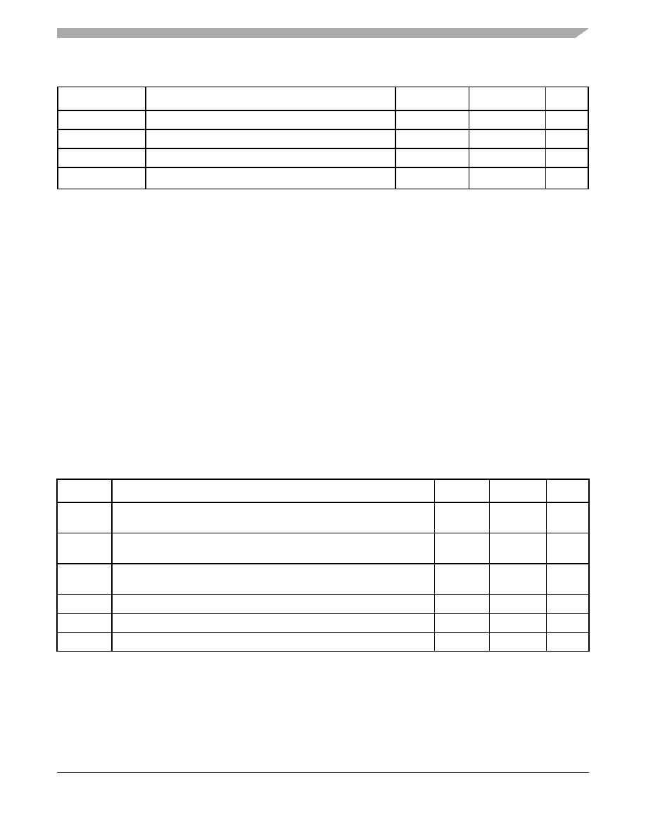
Table 4. Recommended Operating Range
Symbol
Rating
Minimum
Maximum
Unit
TA
Operating temperature range
MC9328MXSVP10
070
°C
TA
Operating temperature range
MC9328MXSCVP10
-40
85
°C
NVDD
I/O supply voltage (if using SPI, LCD, and USBd which are only 3 V
interfaces)
2.70
3.30
V
NVDD
I/O supply voltage (if not using the peripherals listed above)
1.70
3.30
V
QVDD
Internal supply voltage (Core = 100 MHz)
1.70
1.90
V
AVDD
Analog supply voltage
1.70
3.30
V
Table 3. Maximum Ratings (Continued)
Symbol
Rating
Minimum
Maximum
Unit
相关PDF资料 |
PDF描述 |
|---|---|
| MC94MX21DVKN3R2 | 350 MHz, MICROPROCESSOR, PBGA289 |
| MC9S08FL8CLC | 8-BIT, FLASH, 20 MHz, MICROCONTROLLER, QFP32 |
| MC9S08FL8CBM | 8-BIT, FLASH, 20 MHz, MICROCONTROLLER, PDIP32 |
| MC9S08FL16CBM | 8-BIT, FLASH, 20 MHz, MICROCONTROLLER, PDIP32 |
| MC9S08GW64CLH | MICROCONTROLLER, PQFP64 |
相关代理商/技术参数 |
参数描述 |
|---|---|
| MC9328MXSVP10 | 功能描述:处理器 - 专门应用 REDUCED FEATURE CORSICA RoHS:否 制造商:Freescale Semiconductor 类型:Multimedia Applications 核心:ARM Cortex A9 处理器系列:i.MX6 数据总线宽度:32 bit 最大时钟频率:1 GHz 指令/数据缓存: 数据 RAM 大小:128 KB 数据 ROM 大小: 工作电源电压: 最大工作温度:+ 95 C 安装风格:SMD/SMT 封装 / 箱体:MAPBGA-432 |
| MC9328MXSVP10 | 制造商:Freescale Semiconductor 功能描述:Microprocessor |
| MC9328MXSVP10R2 | 功能描述:处理器 - 专门应用 REDUCED FEATURE CORSICA RoHS:否 制造商:Freescale Semiconductor 类型:Multimedia Applications 核心:ARM Cortex A9 处理器系列:i.MX6 数据总线宽度:32 bit 最大时钟频率:1 GHz 指令/数据缓存: 数据 RAM 大小:128 KB 数据 ROM 大小: 工作电源电压: 最大工作温度:+ 95 C 安装风格:SMD/SMT 封装 / 箱体:MAPBGA-432 |
| MC932L | 制造商:Rochester Electronics LLC 功能描述:- Bulk |
| MC933 | 制造商:FREESCALE 制造商全称:Freescale Semiconductor, Inc 功能描述:INTEGRATED CIRCUITS |
发布紧急采购,3分钟左右您将得到回复。