- 您现在的位置:买卖IC网 > PDF目录69031 > MC9S08QE4CPG (FREESCALE SEMICONDUCTOR INC) 8-BIT, FLASH, 20 MHz, MICROCONTROLLER, PDIP16 PDF资料下载
参数资料
| 型号: | MC9S08QE4CPG |
| 厂商: | FREESCALE SEMICONDUCTOR INC |
| 元件分类: | 微控制器/微处理器 |
| 英文描述: | 8-BIT, FLASH, 20 MHz, MICROCONTROLLER, PDIP16 |
| 封装: | ROHS COMPLIANT, PLASTIC, DIP-16 |
| 文件页数: | 1/46页 |
| 文件大小: | 1293K |
| 代理商: | MC9S08QE4CPG |
当前第1页第2页第3页第4页第5页第6页第7页第8页第9页第10页第11页第12页第13页第14页第15页第16页第17页第18页第19页第20页第21页第22页第23页第24页第25页第26页第27页第28页第29页第30页第31页第32页第33页第34页第35页第36页第37页第38页第39页第40页第41页第42页第43页第44页第45页第46页
Freescale Semiconductor
Data Sheet: Technical Data
Document Number: MC9S08QE8
Rev. 7, 4/2009
Freescale Semiconductor, Inc., 2007-2009. All rights reserved.
This document contains information on a product under development. Freescale reserves the
right to change or discontinue this product without notice.
MC9S08QE8
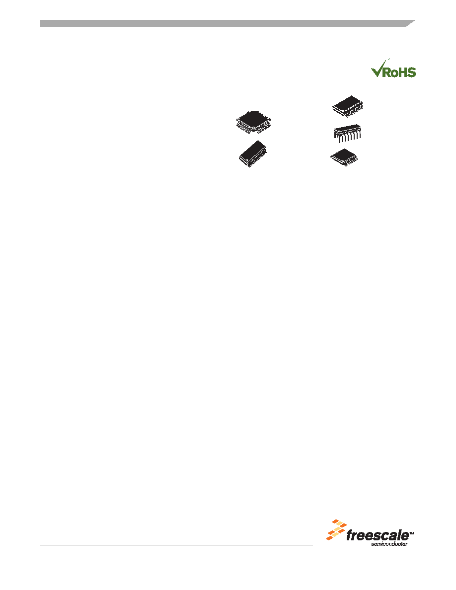
32-Pin LQFP
Case 873A
28-Pin SOIC
751F-05
16-Pin PDIP
648
16-Pin TSSOP
948F
20-Pin SOIC
751D-07
Features
8-Bit HCS08 Central Processor Unit (CPU)
– Up to 20 MHz CPU at 3.6 V to 1.8 V across temperature range of
–40 °C to 85 °C
– HC08 instruction set with added BGND instruction
– Support for up to 32 interrupt/reset sources
On-Chip Memory
– Flash read/program/erase over full operating voltage and
temperature
– Random-access memory (RAM)
– Security circuitry to prevent unauthorized access to RAM and
flash contents
Power-Saving Modes
– Two low power stop modes
– Reduced power wait mode
– Low power run and wait modes allow peripherals to run while
voltage regulator is in standby
– Peripheral clock gating register can disable clocks to unused
modules, thereby reducing currents
– Very low power external oscillator that can be used in stop2 or
stop3 modes to provide accurate clock source to real time counter
–6
μs typical wake-up time from stop3 mode
Clock Source Options
– Oscillator (XOSC) — Loop-control Pierce oscillator; crystal or
ceramic resonator range of 31.25 kHz to 38.4 kHz or 1 MHz to
16 MHz
– Internal Clock Source (ICS) — Internal clock source module
containing a frequency-locked-loop (FLL) controlled by internal
or external reference; precision trimming of internal reference
allows 0.2% resolution and 2% deviation over temperature and
voltage; supporting bus frequencies from 1 MHz to 10 MHz
System Protection
– Watchdog computer operating properly (COP) reset with option to
run from dedicated 1 kHz internal clock source or bus clock
– Low-voltage warning with interrupt
– Low-voltage detection with reset or interrupt
– Illegal opcode detection with reset
– Illegal address detection with reset
– Flash block protection
Development Support
– Single-wire background debug interface
– Breakpoint capability to allow single breakpoint setting during
in-circuit debugging (plus two more breakpoints in on-chip debug
module)
– On-chip in-circuit emulator (ICE) debug module containing two
comparators and nine trigger modes; eight deep FIFO for storing
change-of-flow addresses and event-only data; debug module
supports both tag and force breakpoints
Peripherals
– ADC — 10-channel, 12-bit resolution; 2.5
μs conversion time;
automatic compare function; 1.7 mV/
°C temperature sensor;
internal bandgap reference channel; operation in stop3; fully
functional from 3.6 V to 1.8 V
– ACMPx — Two analog comparators with selectable interrupt on
rising, falling, or either edge of comparator output; compare
option to fixed internal bandgap reference voltage; outputs can be
optionally routed to TPM module; operation in stop3
– SCI — Full-duplex non-return to zero (NRZ); LIN master
extended break generation; LIN slave extended break detection;
wake-up on active edge
– SPI — Full-duplex or single-wire bidirectional; double-buffered
transmit and receive; master or slave mode; MSB-first or
LSB-first shifting
– IIC — Up to 100 kbps with maximum bus loading; multi-master
operation; programmable slave address; interrupt driven
byte-by-byte data transfer; supporting broadcast mode and 10-bit
addressing
– TPMx — Two 3-channel (TPM1 and TPM2); selectable input
capture, output compare, or buffered edge- or center-aligned
PWM on each channel
– RTC — (Real-time counter) 8-bit modulus counter with binary or
decimal based prescaler; external clock source for precise time
base, time-of-day, calendar or task scheduling functions; free
running on-chip low power oscillator (1 kHz) for cyclic wakeup
without external components; runs in all MCU modes
Input/Output
– 26 GPIOs, one output-only pin and one input-only pin
– Eight KBI interrupts with selectable polarity
– Hysteresis and configurable pullup device on all input pins;
configurable slew rate and drive strength on all output pins.
Package Options
– 32-pin LQFP, 28-pin SOIC, 20-pin SOIC, 16-pin PDIP,
16-pin TSSOP
Document Number: MC9S08QE8
Rev. 7, 4/2009
MC9S08QE8 Series
Covers: MC9S08QE8 and
MC9S08QE4
相关PDF资料 |
PDF描述 |
|---|---|
| MC9S08QE4CWJ | 8-BIT, FLASH, 20 MHz, MICROCONTROLLER, PDSO20 |
| MC9S08QE4CTG | 8-BIT, FLASH, 20 MHz, MICROCONTROLLER, PDSO16 |
| MC9S08SF4CTG | MICROCONTROLLER, PDSO16 |
| MC9S08SF4CTJ | MICROCONTROLLER, PDSO20 |
| MC9S12A128BCPV | 16-BIT, FLASH, 25 MHz, MICROCONTROLLER, PQFP112 |
相关代理商/技术参数 |
参数描述 |
|---|---|
| MC9S08QE4CTG | 功能描述:8位微控制器 -MCU 4KB FLASH; 512 RAM RoHS:否 制造商:Silicon Labs 核心:8051 处理器系列:C8051F39x 数据总线宽度:8 bit 最大时钟频率:50 MHz 程序存储器大小:16 KB 数据 RAM 大小:1 KB 片上 ADC:Yes 工作电源电压:1.8 V to 3.6 V 工作温度范围:- 40 C to + 105 C 封装 / 箱体:QFN-20 安装风格:SMD/SMT |
| MC9S08QE4CTGR | 功能描述:8位微控制器 -MCU 4K Flash, 256 Ram RoHS:否 制造商:Silicon Labs 核心:8051 处理器系列:C8051F39x 数据总线宽度:8 bit 最大时钟频率:50 MHz 程序存储器大小:16 KB 数据 RAM 大小:1 KB 片上 ADC:Yes 工作电源电压:1.8 V to 3.6 V 工作温度范围:- 40 C to + 105 C 封装 / 箱体:QFN-20 安装风格:SMD/SMT |
| MC9S08QE4CWJ | 功能描述:8位微控制器 -MCU 4KB FLASH; 512 RAM RoHS:否 制造商:Silicon Labs 核心:8051 处理器系列:C8051F39x 数据总线宽度:8 bit 最大时钟频率:50 MHz 程序存储器大小:16 KB 数据 RAM 大小:1 KB 片上 ADC:Yes 工作电源电压:1.8 V to 3.6 V 工作温度范围:- 40 C to + 105 C 封装 / 箱体:QFN-20 安装风格:SMD/SMT |
| MC9S08QE4CWL | 功能描述:8位微控制器 -MCU 4KB FLASH; 512 RAM RoHS:否 制造商:Silicon Labs 核心:8051 处理器系列:C8051F39x 数据总线宽度:8 bit 最大时钟频率:50 MHz 程序存储器大小:16 KB 数据 RAM 大小:1 KB 片上 ADC:Yes 工作电源电压:1.8 V to 3.6 V 工作温度范围:- 40 C to + 105 C 封装 / 箱体:QFN-20 安装风格:SMD/SMT |
| MC9S08QE64CFT | 功能描述:8位微控制器 -MCU 8 BIT, 64K FLASH RoHS:否 制造商:Silicon Labs 核心:8051 处理器系列:C8051F39x 数据总线宽度:8 bit 最大时钟频率:50 MHz 程序存储器大小:16 KB 数据 RAM 大小:1 KB 片上 ADC:Yes 工作电源电压:1.8 V to 3.6 V 工作温度范围:- 40 C to + 105 C 封装 / 箱体:QFN-20 安装风格:SMD/SMT |
发布紧急采购,3分钟左右您将得到回复。