- 您现在的位置:买卖IC网 > PDF目录45291 > MC9S08RG60CFJ (MOTOROLA INC) 8-BIT, FLASH, 8 MHz, MICROCONTROLLER, PQFP32 PDF资料下载
参数资料
| 型号: | MC9S08RG60CFJ |
| 厂商: | MOTOROLA INC |
| 元件分类: | 微控制器/微处理器 |
| 英文描述: | 8-BIT, FLASH, 8 MHz, MICROCONTROLLER, PQFP32 |
| 封装: | LQFP-32 |
| 文件页数: | 125/232页 |
| 文件大小: | 2818K |
| 代理商: | MC9S08RG60CFJ |
第1页第2页第3页第4页第5页第6页第7页第8页第9页第10页第11页第12页第13页第14页第15页第16页第17页第18页第19页第20页第21页第22页第23页第24页第25页第26页第27页第28页第29页第30页第31页第32页第33页第34页第35页第36页第37页第38页第39页第40页第41页第42页第43页第44页第45页第46页第47页第48页第49页第50页第51页第52页第53页第54页第55页第56页第57页第58页第59页第60页第61页第62页第63页第64页第65页第66页第67页第68页第69页第70页第71页第72页第73页第74页第75页第76页第77页第78页第79页第80页第81页第82页第83页第84页第85页第86页第87页第88页第89页第90页第91页第92页第93页第94页第95页第96页第97页第98页第99页第100页第101页第102页第103页第104页第105页第106页第107页第108页第109页第110页第111页第112页第113页第114页第115页第116页第117页第118页第119页第120页第121页第122页第123页第124页当前第125页第126页第127页第128页第129页第130页第131页第132页第133页第134页第135页第136页第137页第138页第139页第140页第141页第142页第143页第144页第145页第146页第147页第148页第149页第150页第151页第152页第153页第154页第155页第156页第157页第158页第159页第160页第161页第162页第163页第164页第165页第166页第167页第168页第169页第170页第171页第172页第173页第174页第175页第176页第177页第178页第179页第180页第181页第182页第183页第184页第185页第186页第187页第188页第189页第190页第191页第192页第193页第194页第195页第196页第197页第198页第199页第200页第201页第202页第203页第204页第205页第206页第207页第208页第209页第210页第211页第212页第213页第214页第215页第216页第217页第218页第219页第220页第221页第222页第223页第224页第225页第226页第227页第228页第229页第230页第231页第232页
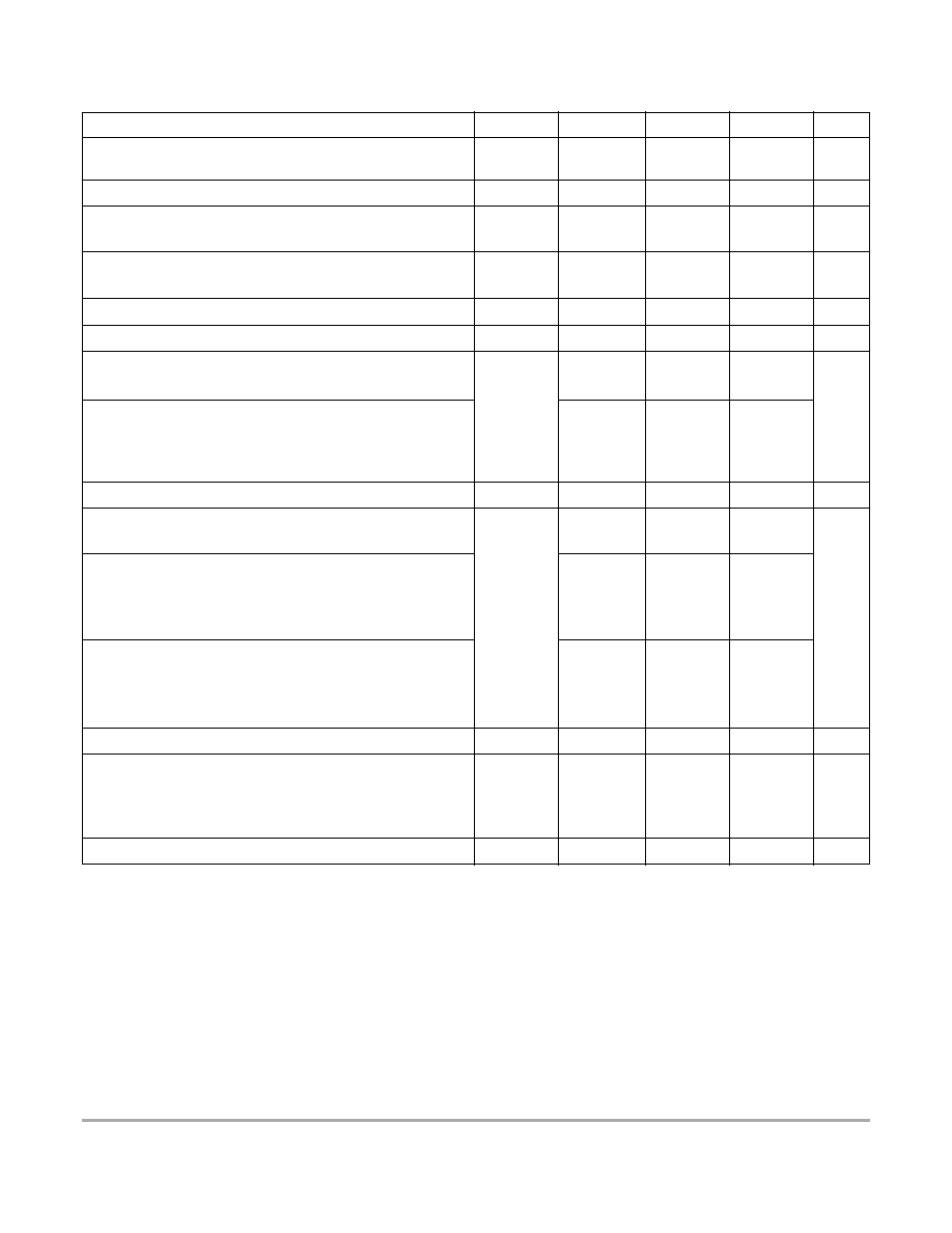
Electrical Characteristics
MC9S08RC/RD/RE/RG
210
MOTOROLA
Input low voltage (1.8 V
≤ V
DD ≤ 2.3 V)
(all digital inputs)
VIL
—
0.30
×
VDD
V
Input hysteresis (all digital inputs)
Vhys
0.06
× V
DD
—V
Input leakage current (Per pin)
VIn = VDD or VSS, all input only pins
|IIn|
—
0.025
1.0
A
High impedance (off-state) leakage current (per pin)
VIn = VDD or VSS, all input/output
|IOZ|
—
0.025
1.0
A
Internal pullup resistors(4) (5)
RPU
17.5
52.5
k
Internal pulldown resistor (IRQ)
RPD
17.5
52.5
k
Output high voltage (VDD ≥ 1.8 V)
IOH = –2 mA (ports A, C, D and E)
VOH
VDD – 0.5
—
V
Output high voltage (port B and IRO)
IOH = –10 mA (VDD ≥ 2.7 V)
IOH = –6 mA (VDD ≥ 2.3 V)
IOH = –3 mA (VDD ≥ 1.8 V)
VDD – 0.5
—
Maximum total IOH for all port pins
|IOHT|
—60
mA
Output low voltage (VDD ≥ 1.8 V)
IOL = 2.0 mA (ports A, C, D and E)
VOL
—
0.5
V
Output low voltage (port B)
IOL = 10.0 mA (VDD ≥ 2.7 V)
IOL = 6 mA (VDD ≥ 2.3 V)
IOL = 3 mA (VDD ≥ 1.8 V)
—
0.5
Output low voltage (IRO)
IOL = 16 mA (VDD ≥ 2.7 V)
IOL =TBD mA (VDD ≥ 2.3 V)
IOL = TBD mA (VDD ≥ 1.8 V)
—
1.2
Maximum total IOL for all port pins
IOLT
—60
mA
dc injection current(2), (6), (7), (8),, (9)
VIN < VSS, VIN > VDD
Single pin limit
Total MCU limit, includes sum of all stressed pins
|IIC|
—
0.2
5
mA
Input capacitance (all non-supply pins)
CIn
—7
pF
NOTES:
1. RAM will retain data down to POR voltage. RAM data not guaranteed to be valid following a POR.
2. This parameter is characterized and not tested on each device.
3. If SAFE bit is set, VDD must be above re-arm voltage to allow MCU to accept interrupts, refer to 5.6 Low-Voltage Detect
4. Measurement condition for pull resistors: VIn = VSS for pullup and VIn = VDD for pulldown.
5. The PTA0 pullup resistor may not pull up to the specified minimum VIH. However, all ports are functionally tested to
guarantee that a logic 1 will be read on any port input when the pullup is enabled and no dc load is present on the pin. In
addition, the test checks that the pin is pulled up from VSS to a logic 1 within 20 s with a nominal capacitance of 75 pF.
6. All functional non-supply pins are internally clamped to VSS and VDD.
7. Input must be current limited to the value specified. To determine the value of the required current-limiting resistor,
calculate resistance values for positive and negative clamp voltages, then use the larger of the two values.
Table A-4 DC Characteristics (Continued)(Temperature Range = –40 to 85
°C Ambient)
Parameter
Symbol
Min
Typical
Max
Unit
相关PDF资料 |
PDF描述 |
|---|---|
| MC9S08RE60CFJ | 8-BIT, FLASH, 8 MHz, MICROCONTROLLER, PQFP32 |
| MC9S08RE32CFJ | 8-BIT, FLASH, 8 MHz, MICROCONTROLLER, PQFP32 |
| MC9S08RD60CPE | 8-BIT, FLASH, 8 MHz, MICROCONTROLLER, PDIP28 |
| MC9S08RE60CFG | 8-BIT, FLASH, 8 MHz, MICROCONTROLLER, PQFP44 |
| MC9S08RD16CFG | 8-BIT, FLASH, 8 MHz, MICROCONTROLLER, PQFP44 |
相关代理商/技术参数 |
参数描述 |
|---|---|
| MC9S08RG60CFJE | 功能描述:8位微控制器 -MCU 9S08 2K RAM 60K FLASH RoHS:否 制造商:Silicon Labs 核心:8051 处理器系列:C8051F39x 数据总线宽度:8 bit 最大时钟频率:50 MHz 程序存储器大小:16 KB 数据 RAM 大小:1 KB 片上 ADC:Yes 工作电源电压:1.8 V to 3.6 V 工作温度范围:- 40 C to + 105 C 封装 / 箱体:QFN-20 安装风格:SMD/SMT |
| MC9S08RG60CFJER | 制造商:Freescale Semiconductor 功能描述:9S08 2K RAM 60K FLASH - Tape and Reel |
| MC9S08RG60CPE | 制造商:FREESCALE 制造商全称:Freescale Semiconductor, Inc 功能描述:Microcontrollers |
| MC9S08RG60DWE | 制造商:FREESCALE 制造商全称:Freescale Semiconductor, Inc 功能描述:Microcontrollers |
| MC9S08RG60FDE | 制造商:FREESCALE 制造商全称:Freescale Semiconductor, Inc 功能描述:Microcontrollers |
发布紧急采购,3分钟左右您将得到回复。