- 您现在的位置:买卖IC网 > PDF目录45298 > MC9S12DB128VFU (FREESCALE SEMICONDUCTOR INC) 16-BIT, FLASH, 25 MHz, MICROCONTROLLER, PQFP80 PDF资料下载
参数资料
| 型号: | MC9S12DB128VFU |
| 厂商: | FREESCALE SEMICONDUCTOR INC |
| 元件分类: | 微控制器/微处理器 |
| 英文描述: | 16-BIT, FLASH, 25 MHz, MICROCONTROLLER, PQFP80 |
| 封装: | PLASTIC, LQFP-80 |
| 文件页数: | 142/142页 |
| 文件大小: | 6464K |
| 代理商: | MC9S12DB128VFU |
第1页第2页第3页第4页第5页第6页第7页第8页第9页第10页第11页第12页第13页第14页第15页第16页第17页第18页第19页第20页第21页第22页第23页第24页第25页第26页第27页第28页第29页第30页第31页第32页第33页第34页第35页第36页第37页第38页第39页第40页第41页第42页第43页第44页第45页第46页第47页第48页第49页第50页第51页第52页第53页第54页第55页第56页第57页第58页第59页第60页第61页第62页第63页第64页第65页第66页第67页第68页第69页第70页第71页第72页第73页第74页第75页第76页第77页第78页第79页第80页第81页第82页第83页第84页第85页第86页第87页第88页第89页第90页第91页第92页第93页第94页第95页第96页第97页第98页第99页第100页第101页第102页第103页第104页第105页第106页第107页第108页第109页第110页第111页第112页第113页第114页第115页第116页第117页第118页第119页第120页第121页第122页第123页第124页第125页第126页第127页第128页第129页第130页第131页第132页第133页第134页第135页第136页第137页第138页第139页第140页第141页当前第142页
Device User Guide — 9S12DT128DGV2/D V02.15
99
Freescale Semiconductor
A.1.5 Absolute Maximum Ratings
Absolute maximum ratings are stress ratings only. A functional operation under or outside those maxima
is not guaranteed. Stress beyond those limits may affect the reliability or cause permanent damage of the
device.
This device contains circuitry protecting against damage due to high static voltage or electrical fields;
however, it is advised that normal precautions be taken to avoid application of any voltages higher than
maximum-rated voltages to this high-impedance circuit. Reliability of operation is enhanced if unused
inputs are tied to an appropriate logic voltage level (e.g., either VSS5 or VDD5).
A.1.6 ESD Protection and Latch-up Immunity
All ESD testing is in conformity with CDF-AEC-Q100 Stress test qualification for Automotive Grade
Integrated Circuits. During the device qualification ESD stresses were performed for the Human Body
Model (HBM), the Machine Model (MM) and the Charge Device Model.
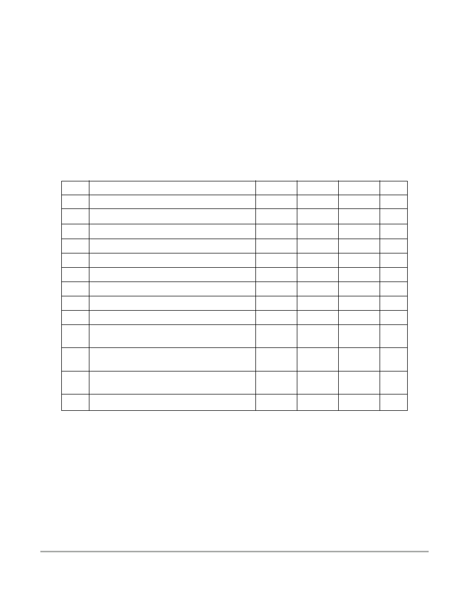
Table A-1 Absolute Maximum Ratings1
NOTES:
1. Beyond absolute maximum ratings device might be damaged.
Num
Rating
Symbol
Min
Max
Unit
1
I/O, Regulator and Analog Supply Voltage
VDD5
-0.3
6.0
V
2
Digital Logic Supply Voltage 2
2. The device contains an internal voltage regulator to generate the logic and PLL supply out of the I/O supply.
The absolute maximum ratings apply when the device is powered from an external source.
VDD
-0.3
3.0
V
3
PLL Supply Voltage (2)
VDDPLL
-0.3
3.0
V
4
Voltage difference VDDX to VDDR and VDDA
VDDX
-0.3
0.3
V
5
Voltage difference VSSX to VSSR and VSSA
VSSX
-0.3
0.3
V
6
Digital I/O Input Voltage
VIN
-0.3
6.0
V
7
Analog Reference
VRH, VRL
-0.3
6.0
V
8
XFC, EXTAL, XTAL inputs
VILV
-0.3
3.0
V
9
TEST input
VTEST
-0.3
10.0
V
10
Instantaneous Maximum Current
Single pin limit for all digital I/O pins 3
3. All digital I/O pins are internally clamped to VSSX and VDDX, VSSR and VDDR or VSSA and VDDA.
I
D
-25
+25
mA
11
Instantaneous Maximum Current
Single pin limit for XFC, EXTAL, XTAL4
4. Those pins are internally clamped to VSSPLL and VDDPLL.
I
DL
-25
+25
mA
12
Instantaneous Maximum Current
Single pin limit for TEST 5
5. This pin is clamped low to VSSX, but not clamped high. This pin must be tied low in applications.
I
DT
-0.25
0
mA
13
Storage Temperature Range
T
stg
– 65
155
°C
相关PDF资料 |
PDF描述 |
|---|---|
| MC9S12DG128CFUR2 | 16-BIT, FLASH, 25 MHz, MICROCONTROLLER, PQFP80 |
| MC9S12DG128MFUR2 | 16-BIT, FLASH, 25 MHz, MICROCONTROLLER, PQFP80 |
| MC9S12DJ128MPV | 16-BIT, FLASH, 25 MHz, MICROCONTROLLER, PQFP112 |
| MC9S12DG128ECFU | 16-BIT, FLASH, 25 MHz, MICROCONTROLLER, PQFP80 |
| MC9S12DG128VFU | 16-BIT, FLASH, 25 MHz, MICROCONTROLLER, PQFP80 |
相关代理商/技术参数 |
参数描述 |
|---|---|
| MC9S12DB128VPVE | 功能描述:16位微控制器 - MCU MARLIN2 PB FREE RoHS:否 制造商:Texas Instruments 核心:RISC 处理器系列:MSP430FR572x 数据总线宽度:16 bit 最大时钟频率:24 MHz 程序存储器大小:8 KB 数据 RAM 大小:1 KB 片上 ADC:Yes 工作电源电压:2 V to 3.6 V 工作温度范围:- 40 C to + 85 C 封装 / 箱体:VQFN-40 安装风格:SMD/SMT |
| MC9S12DG128BCFU | 功能描述:16位微控制器 - MCU 16 Bit 25MHz RoHS:否 制造商:Texas Instruments 核心:RISC 处理器系列:MSP430FR572x 数据总线宽度:16 bit 最大时钟频率:24 MHz 程序存储器大小:8 KB 数据 RAM 大小:1 KB 片上 ADC:Yes 工作电源电压:2 V to 3.6 V 工作温度范围:- 40 C to + 85 C 封装 / 箱体:VQFN-40 安装风格:SMD/SMT |
| MC9S12DG128BCPV | 功能描述:16位微控制器 - MCU 16 Bit 25MHz RoHS:否 制造商:Texas Instruments 核心:RISC 处理器系列:MSP430FR572x 数据总线宽度:16 bit 最大时钟频率:24 MHz 程序存储器大小:8 KB 数据 RAM 大小:1 KB 片上 ADC:Yes 工作电源电压:2 V to 3.6 V 工作温度范围:- 40 C to + 85 C 封装 / 箱体:VQFN-40 安装风格:SMD/SMT |
| MC9S12DG128BMFU | 制造商:Rochester Electronics LLC 功能描述:- Bulk |
| MC9S12DG128BVFU | 功能描述:16位微控制器 - MCU 16 Bit 25MHz RoHS:否 制造商:Texas Instruments 核心:RISC 处理器系列:MSP430FR572x 数据总线宽度:16 bit 最大时钟频率:24 MHz 程序存储器大小:8 KB 数据 RAM 大小:1 KB 片上 ADC:Yes 工作电源电压:2 V to 3.6 V 工作温度范围:- 40 C to + 85 C 封装 / 箱体:VQFN-40 安装风格:SMD/SMT |
发布紧急采购,3分钟左右您将得到回复。