- 您现在的位置:买卖IC网 > PDF目录45311 > MCF5274VM166 (FREESCALE SEMICONDUCTOR INC) 32-BIT, 166 MHz, RISC PROCESSOR, PBGA256 PDF资料下载
参数资料
| 型号: | MCF5274VM166 |
| 厂商: | FREESCALE SEMICONDUCTOR INC |
| 元件分类: | 微控制器/微处理器 |
| 英文描述: | 32-BIT, 166 MHz, RISC PROCESSOR, PBGA256 |
| 封装: | ROHS COMPLIANT, PLASTIC, MAPBGA-256 |
| 文件页数: | 17/44页 |
| 文件大小: | 980K |
| 代理商: | MCF5274VM166 |
第1页第2页第3页第4页第5页第6页第7页第8页第9页第10页第11页第12页第13页第14页第15页第16页当前第17页第18页第19页第20页第21页第22页第23页第24页第25页第26页第27页第28页第29页第30页第31页第32页第33页第34页第35页第36页第37页第38页第39页第40页第41页第42页第43页第44页
MCF5275 Integrated Microprocessor Family Hardware Specification, Rev. 4
Electrical Characteristics
Freescale Semiconductor
24
8.6
External Interface Timing Characteristics
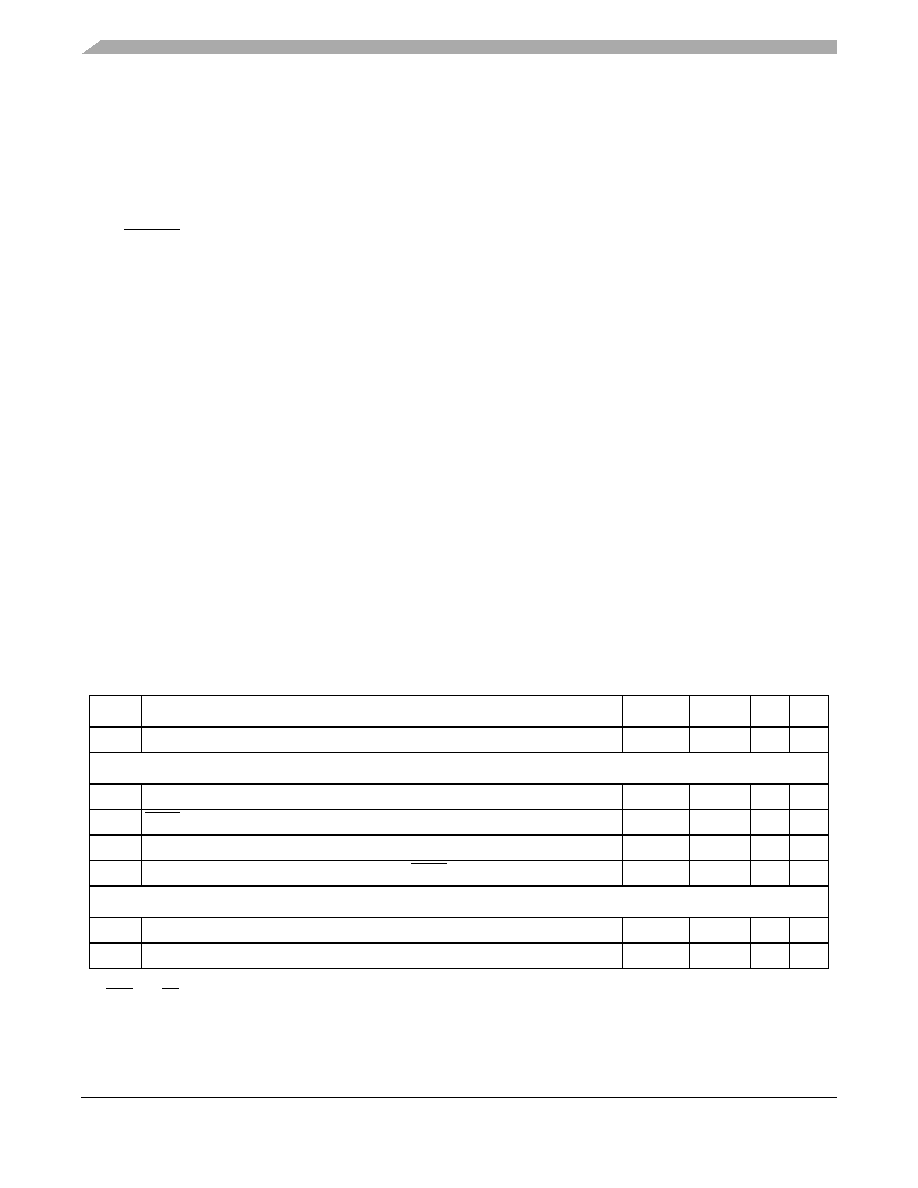
Table 12 lists processor bus input timings.
NOTE
All processor bus timings are synchronous; that is, input setup/hold and
output delay with respect to the rising edge of a reference clock. The
reference clock is the CLKOUT output.
All other timing relationships can be derived from these values.
4
Self clocked mode frequency is the frequency that the PLL operates at when the reference frequency falls below
fLOR with default MFD/RFD settings.
5
This parameter is guaranteed by characterization before qualification rather than 100% tested.
6
Proper PC board layout procedures must be followed to achieve specifications.
7
Load capacitance determined from crystal manufacturer specifications and includes circuit board parasitics.
8
This specification applies to the period required for the PLL to relock after changing the MFD frequency control bits
in the synthesizer control register (SYNCR).
9
Assuming a reference is available at power up, lock time is measured from the time VDD and VDDPLL are valid to
RSTOUT negating. If the crystal oscillator is being used as the reference for the PLL, then the crystal start up time
must be added to the PLL lock time to determine the total start-up time.
10 t
lpll = (64 * 4 * 5 + 5 x τ) x Tref, where Tref = 1/Fref_crystal = 1/Fref_ext = 1/Fref_1:1, and τ = 1.57x10
-6 x 2(MFD + 2)
11 PLL is operating in 1:1 PLL mode.
12 Jitter is the average deviation from the programmed frequency measured over the specified interval at maximum
fsys/2. Measurements are made with the device powered by filtered supplies and clocked by a stable external clock
signal. Noise injected into the PLL circuitry via VDDPLL and VSSPLL and variation in crystal oscillator frequency
increase the jitter percentage for a given interval.
13 Based on slow system clock of 33MHz maximum frequency.
14 Modulation percentage applies over an interval of 10
μs, or equivalently the modulation rate is 100KHz.
15 Modulation rate selected must not result in f
sys/2 value greater than the fsys/2 maximum specified value. Modulation
range determined by hardware design.
16 f
sys/2 = fico / (2 * 2
RFD)
Table 12. Processor Bus Input Timing Specifications
Name
Characteristic1
1
Timing specifications have been indicated taking into account the full drive strength for the pads.
Symbol
Min
Max
Unit
B0
CLKOUT
tCYC
12
—
ns
Control Inputs
B1a
Control input valid to CLKOUT high2
2
TEA and TA pins are being referred to as control inputs.
tCVCH
9—
ns
B1b
BKPT valid to CLKOUT high3
3
Refer to figure A-19.
tBKVCH
9—
ns
B2a
CLKOUT high to control inputs invalid2
tCHCII
0—
ns
B2b
CLKOUT high to asynchronous control input BKPT invalid3
tBKNCH
0—
ns
Data Inputs
B4
Data input (D[31:16]) valid to CLKOUT high
tDIVCH
4—
ns
B5
CLKOUT high to data input (D[31:16]) invalid
tCHDII
0—
ns
Because
of
an
order
from
the
United
States
International
Trade
Commission,
BGA-packaged
product
lines
and
part
numbers
indicated
here
currently
are
not
available
from
Freescale
for
import
or
sale
in
the
United
States
prior
to
September
2010:
M5275EVB,
MCF5274CVM166,
MCF5274LCVM166,
MCF5274LVM166,
MCF5274VM166,
MCF5275CVM166,
MCF5275LCVM166
相关PDF资料 |
PDF描述 |
|---|---|
| MCF5275LCVM133 | 32-BIT, 133 MHz, RISC PROCESSOR, PBGA196 |
| MCF5275CVM133 | 32-BIT, 133 MHz, RISC PROCESSOR, PBGA256 |
| MCF5274VM133 | 32-BIT, 133 MHz, RISC PROCESSOR, PBGA256 |
| MCF5280CVF80 | FLASH, 80 MHz, RISC MICROCONTROLLER, PBGA256 |
| MCF5281CVM80 | FLASH, 80 MHz, RISC MICROCONTROLLER, PBGA256 |
相关代理商/技术参数 |
参数描述 |
|---|---|
| MCF5274VM166J | 制造商:Freescale Semiconductor 功能描述:MCF5274 V2CORE 64KSRAM - Bulk |
| MCF5275 | 制造商:FREESCALE 制造商全称:Freescale Semiconductor, Inc 功能描述:Integrated Microprocessor Family Hardware Specification |
| MCF5275CVM133 | 功能描述:IC MCU 32BIT 133MHZ 256-MAPBGA RoHS:否 类别:集成电路 (IC) >> 嵌入式 - 微控制器, 系列:MCF527x 标准包装:250 系列:56F8xxx 核心处理器:56800E 芯体尺寸:16-位 速度:60MHz 连通性:CAN,SCI,SPI 外围设备:POR,PWM,温度传感器,WDT 输入/输出数:21 程序存储器容量:40KB(20K x 16) 程序存储器类型:闪存 EEPROM 大小:- RAM 容量:6K x 16 电压 - 电源 (Vcc/Vdd):2.25 V ~ 3.6 V 数据转换器:A/D 6x12b 振荡器型:内部 工作温度:-40°C ~ 125°C 封装/外壳:48-LQFP 包装:托盘 配用:MC56F8323EVME-ND - BOARD EVALUATION MC56F8323 |
| MCF5275CVM166 | 功能描述:微处理器 - MPU MCF5275 V2CORE 64KSRAM RoHS:否 制造商:Atmel 处理器系列:SAMA5D31 核心:ARM Cortex A5 数据总线宽度:32 bit 最大时钟频率:536 MHz 程序存储器大小:32 KB 数据 RAM 大小:128 KB 接口类型:CAN, Ethernet, LIN, SPI,TWI, UART, USB 工作电源电压:1.8 V to 3.3 V 最大工作温度:+ 85 C 安装风格:SMD/SMT 封装 / 箱体:FBGA-324 |
| MCF5275CVM166 | 制造商:Freescale Semiconductor 功能描述:Microprocessor IC |
发布紧急采购,3分钟左右您将得到回复。