- 您现在的位置:买卖IC网 > PDF目录10951 > MCF5329CVM240J (Freescale Semiconductor)IC MPU RISC 240MHZ 256MAPBGA PDF资料下载
参数资料
| 型号: | MCF5329CVM240J |
| 厂商: | Freescale Semiconductor |
| 文件页数: | 13/50页 |
| 文件大小: | 0K |
| 描述: | IC MPU RISC 240MHZ 256MAPBGA |
| 标准包装: | 90 |
| 系列: | MCF532x |
| 核心处理器: | Coldfire V3 |
| 芯体尺寸: | 32-位 |
| 速度: | 240MHz |
| 连通性: | CAN,EBI/EMI,以太网,I²C,SPI,SSI,UART/USART,USB,USB OTG |
| 外围设备: | DMA,LCD,PWM,WDT |
| 输入/输出数: | 94 |
| 程序存储器类型: | ROMless |
| RAM 容量: | 32K x 8 |
| 电压 - 电源 (Vcc/Vdd): | 1.4 V ~ 3.6 V |
| 振荡器型: | 外部 |
| 工作温度: | -40°C ~ 85°C |
| 封装/外壳: | 256-LBGA |
| 包装: | 托盘 |
第1页第2页第3页第4页第5页第6页第7页第8页第9页第10页第11页第12页当前第13页第14页第15页第16页第17页第18页第19页第20页第21页第22页第23页第24页第25页第26页第27页第28页第29页第30页第31页第32页第33页第34页第35页第36页第37页第38页第39页第40页第41页第42页第43页第44页第45页第46页第47页第48页第49页第50页
MCF532x ColdFire Microprocessor Data Sheet, Rev. 5
Electrical Characteristics
Freescale Semiconductor
20
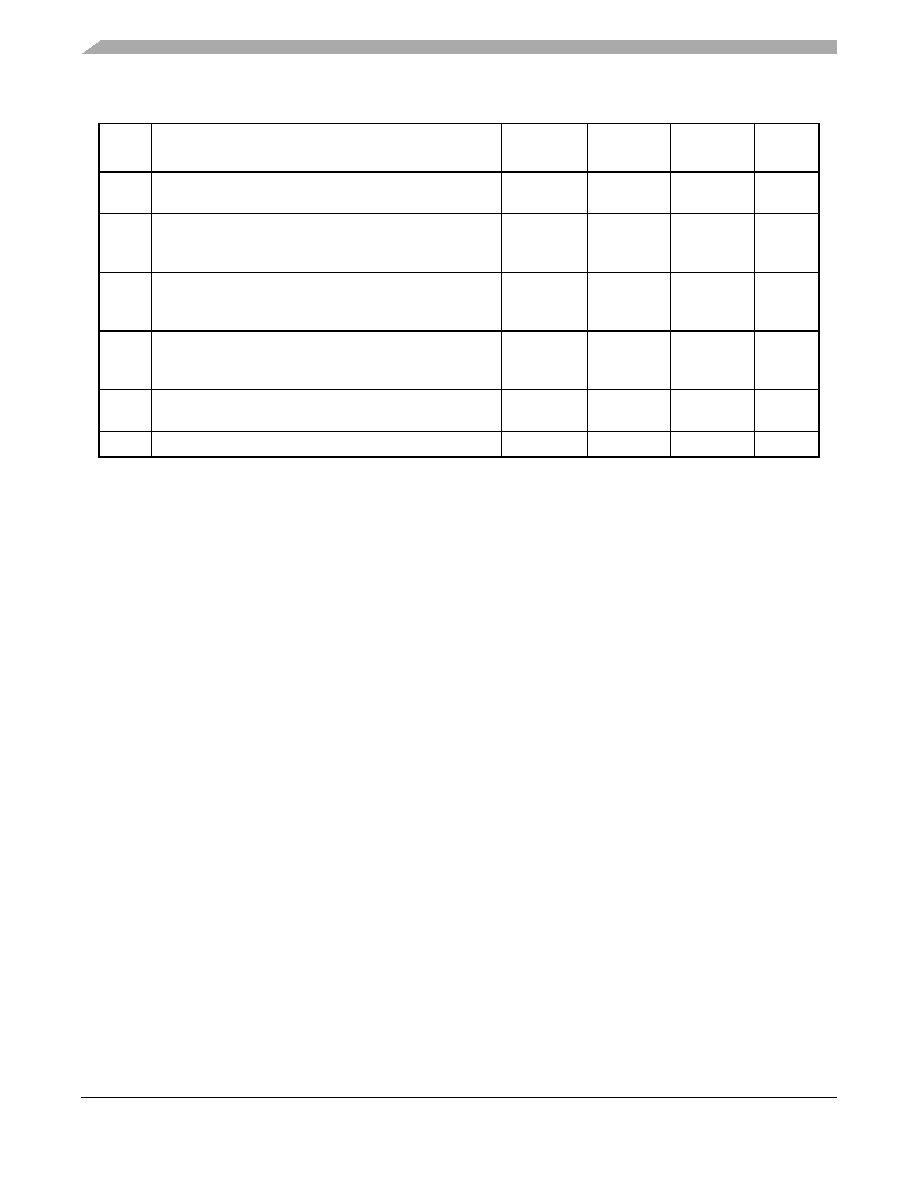
5.6
External Interface Timing Characteristics
Table 9 lists processor bus input timings.
NOTE
All processor bus timings are synchronous; that is, input setup/hold and output delay with
respect to the rising edge of a reference clock. The reference clock is the FB_CLK output.
All other timing relationships can be derived from these values. Timings listed in Table 9
12
Crystal capacitive load
CL
See crystal
spec
13
Discrete load capacitance for XTAL
CL_XTAL
2*CL –
CS_XTAL –
CPCB_XTAL
7
pF
14
Discrete load capacitance for EXTAL
CL_EXTAL
2*CL–-
CS_EXTAL –
CPCB_EXTAL
pF
17
Peak-to-peak Jitter (Clock edge to clock edge)
Long Term Jitter
Cjitter
—
10
TBD
% fsys/3
18
Frequency Modulation Range Limit 3, 10, 11
(fsysMax must not be exceeded)
Cmod
0.8
2.2
%fsys/3
19
VCO Frequency. fvco = (fref * PFD)/4
fvco
350
540
MHz
1 The maximum allowable input clock frequency when booting with the PLL enabled is 24MHz. For higher input clock
frequencies the processor must boot in LIMP mode to avoid violating the maximum allowable CPU frequency.
2 All internal registers retain data at 0 Hz.
3 This parameter is guaranteed by characterization before qualification rather than 100% tested.
4 Proper PC board layout procedures must be followed to achieve specifications.
5 This parameter is guaranteed by design rather than 100% tested.
6 This specification is the PLL lock time only and does not include oscillator start-up time.
7 C
PCB_EXTAL and CPCB_XTAL are the measured PCB stray capacitances on EXTAL and XTAL, respectively.
8 Jitter is the average deviation from the programmed frequency measured over the specified interval at maximum f
sys.
Measurements are made with the device powered by filtered supplies and clocked by a stable external clock signal.
Noise injected into the PLL circuitry via PLL VDD, EVDD, and VSS and variation in crystal oscillator frequency increase
the Cjitter percentage for a given interval.
9 Values are with frequency modulation disabled. If frequency modulation is enabled, jitter is the sum of Cjitter+Cmod.
10 Modulation percentage applies over an interval of 10
μs, or equivalently the modulation rate is 100 KHz.
11 Modulation range determined by hardware design.
Table 8. PLL Electrical Characteristics (continued)
Num
Characteristic
Symbol
Min.
Value
Max.
Value
Unit
相关PDF资料 |
PDF描述 |
|---|---|
| VI-26J-IY-F4 | CONVERTER MOD DC/DC 36V 50W |
| VI-26J-IY-F2 | CONVERTER MOD DC/DC 36V 50W |
| MC9328MXLVM15R2 | IC MCU I.MX 150MHZ 256-MAPBGA |
| VI-26D-IY-F2 | CONVERTER MOD DC/DC 85V 50W |
| VI-26B-IY-F2 | CONVERTER MOD DC/DC 95V 50W |
相关代理商/技术参数 |
参数描述 |
|---|---|
| MCF5329DS | 制造商:ANALOGICTECH 制造商全称:Advanced Analogic Technologies 功能描述:MCF5329 ColdFire Microprocessor Data Sheet |
| MCF5372 | 制造商:FREESCALE 制造商全称:Freescale Semiconductor, Inc 功能描述:ColdFire㈢ Microprocessor |
| MCF53721 | 制造商:FREESCALE 制造商全称:Freescale Semiconductor, Inc 功能描述:ColdFire㈢ Microprocessor |
| MCF53721CVM240 | 功能描述:微处理器 - MPU MCF5329 DRAGONFIRE RoHS:否 制造商:Atmel 处理器系列:SAMA5D31 核心:ARM Cortex A5 数据总线宽度:32 bit 最大时钟频率:536 MHz 程序存储器大小:32 KB 数据 RAM 大小:128 KB 接口类型:CAN, Ethernet, LIN, SPI,TWI, UART, USB 工作电源电压:1.8 V to 3.3 V 最大工作温度:+ 85 C 安装风格:SMD/SMT 封装 / 箱体:FBGA-324 |
| MCF5372CAB180 | 制造商:FREESCALE 制造商全称:Freescale Semiconductor, Inc 功能描述:Microprocessor Data Sheet |
发布紧急采购,3分钟左右您将得到回复。