- 您现在的位置:买卖IC网 > PDF目录224201 > MCH908JW32FC (FREESCALE SEMICONDUCTOR INC) 8-BIT, FLASH, 8 MHz, MICROCONTROLLER, QCC48 PDF资料下载
参数资料
| 型号: | MCH908JW32FC |
| 厂商: | FREESCALE SEMICONDUCTOR INC |
| 元件分类: | 微控制器/微处理器 |
| 英文描述: | 8-BIT, FLASH, 8 MHz, MICROCONTROLLER, QCC48 |
| 封装: | QFN-48 |
| 文件页数: | 197/228页 |
| 文件大小: | 1433K |
| 代理商: | MCH908JW32FC |
第1页第2页第3页第4页第5页第6页第7页第8页第9页第10页第11页第12页第13页第14页第15页第16页第17页第18页第19页第20页第21页第22页第23页第24页第25页第26页第27页第28页第29页第30页第31页第32页第33页第34页第35页第36页第37页第38页第39页第40页第41页第42页第43页第44页第45页第46页第47页第48页第49页第50页第51页第52页第53页第54页第55页第56页第57页第58页第59页第60页第61页第62页第63页第64页第65页第66页第67页第68页第69页第70页第71页第72页第73页第74页第75页第76页第77页第78页第79页第80页第81页第82页第83页第84页第85页第86页第87页第88页第89页第90页第91页第92页第93页第94页第95页第96页第97页第98页第99页第100页第101页第102页第103页第104页第105页第106页第107页第108页第109页第110页第111页第112页第113页第114页第115页第116页第117页第118页第119页第120页第121页第122页第123页第124页第125页第126页第127页第128页第129页第130页第131页第132页第133页第134页第135页第136页第137页第138页第139页第140页第141页第142页第143页第144页第145页第146页第147页第148页第149页第150页第151页第152页第153页第154页第155页第156页第157页第158页第159页第160页第161页第162页第163页第164页第165页第166页第167页第168页第169页第170页第171页第172页第173页第174页第175页第176页第177页第178页第179页第180页第181页第182页第183页第184页第185页第186页第187页第188页第189页第190页第191页第192页第193页第194页第195页第196页当前第197页第198页第199页第200页第201页第202页第203页第204页第205页第206页第207页第208页第209页第210页第211页第212页第213页第214页第215页第216页第217页第218页第219页第220页第221页第222页第223页第224页第225页第226页第227页第228页
Clock Generator Module (CGM)
MC68HC908JW32 Data Sheet, Rev. 3
70
Freescale Semiconductor
BCS — Base Clock Select Bit
This read/write bit selects either the oscillator output, CGMXCLK, or the VCO clock, CGMVCLK, as
the source of the CGM output, CGMOUT. CGMOUT frequency is one-half the frequency of the
selected clock. BCS cannot be set while the PLLON bit is clear. After toggling BCS, it may take up to
three CGMXCLK and three CGMVCLK cycles to complete the transition from one source clock to the
other. During the transition, CGMOUT is held in stasis. (See 5.3.8 Base Clock Selector Circuit.) Reset
clears the BCS bit.
1 = CGMVCLK divided by three drives CGMOUT
0 = CGMXCLK divided by two drives CGMOUT
NOTE
PLLON and BCS have built-in protection that prevents the base clock
selector circuit from selecting the VCO clock as the source of the base clock
if the PLL is off. Therefore, PLLON cannot be cleared when BCS is set, and
BCS cannot be set when PLLON is clear. If the PLL is off (PLLON = 0),
selecting CGMVCLK requires two writes to the PLL control register. (See
PRE1 and PRE0 — Prescaler Program Bits
These read/write bits control a prescaler that selects the prescaler power-of-two multiplier, P. (See
5.3.3 PLL Circuits and 5.3.6 Programming the PLL.) PRE1 and PRE0 cannot be written when the
PLLON bit is set. Reset clears these bits.
These prescaler bits affects the relationship between the VCO clock and the final system bus clock.
VPR1 and VPR0 — VCO Power-of-Two Range Select Bits
These read/write bits control the VCO’s hardware power-of-two range multiplier E that, in conjunction
Register.) controls the hardware center-of-range frequency, f
VRS. VPR1:VPR0 cannot be written when
the PLLON bit is set. Reset clears these bits.
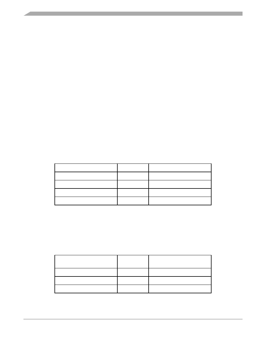
Table 5-2. PRE1 and PRE0 Programming
PRE1 and PRE0
P
Prescaler Multiplier
00
0
1
01
1
2
10
2
4
11
3
8
Table 5-3. VPR1 and VPR0 Programming
VPR1 and VPR0
E
VCO Power-of-Two
Range Multiplier
00
0
1
01
1
2
10
2
4
NOTE: Do not program E to a value of 3.
相关PDF资料 |
PDF描述 |
|---|---|
| MCK-RKHT-043 | SIP43, IC SOCKET |
| MCK-AHGG-001 | SIP1, IC SOCKET |
| MCK-AHGG-004 | SIP4, IC SOCKET |
| MCK-AHGG-005 | SIP5, IC SOCKET |
| MCK-AHGG-008 | SIP8, IC SOCKET |
相关代理商/技术参数 |
参数描述 |
|---|---|
| MCH-BUTTON-LP4 | 功能描述:MEMORY CARD HEADER RoHS:否 类别:连接器,互连式 >> 存储器 - PC 卡 - 连接器 系列:- 产品目录绘图:67600-8001 标准包装:1 系列:67600 卡类型:安全数字式 - SD 位置数:12(9 + 3) 连接器类型:连接器和弹出器 插入,移除方法:推入式,推出式 弹出器侧:- 安装类型:表面贴装,直角 特点:开关 板上方高度:0.110"(2.80mm) 安装特点:正常,标准 - 顶部 包装:Digi-Reel® 触点表面涂层:金 触点涂层厚度:2µin(0.05µm) 其它名称:WM19017DKR |
| MCHC11F1CFNE2 | 功能描述:8位微控制器 -MCU 8B MCU 1KRAM 512EE RoHS:否 制造商:Silicon Labs 核心:8051 处理器系列:C8051F39x 数据总线宽度:8 bit 最大时钟频率:50 MHz 程序存储器大小:16 KB 数据 RAM 大小:1 KB 片上 ADC:Yes 工作电源电压:1.8 V to 3.6 V 工作温度范围:- 40 C to + 105 C 封装 / 箱体:QFN-20 安装风格:SMD/SMT |
| MCHC11F1CFNE2 | 制造商:Freescale Semiconductor 功能描述:8-Bit Microcontroller IC |
| MCHC11F1CFNE2R | 功能描述:8位微控制器 -MCU 8B MCU 1KRAM 512EE RoHS:否 制造商:Silicon Labs 核心:8051 处理器系列:C8051F39x 数据总线宽度:8 bit 最大时钟频率:50 MHz 程序存储器大小:16 KB 数据 RAM 大小:1 KB 片上 ADC:Yes 工作电源电压:1.8 V to 3.6 V 工作温度范围:- 40 C to + 105 C 封装 / 箱体:QFN-20 安装风格:SMD/SMT |
| MCHC11F1CFNE3 | 功能描述:8位微控制器 -MCU 8B MCU 1KRAM 512EE RoHS:否 制造商:Silicon Labs 核心:8051 处理器系列:C8051F39x 数据总线宽度:8 bit 最大时钟频率:50 MHz 程序存储器大小:16 KB 数据 RAM 大小:1 KB 片上 ADC:Yes 工作电源电压:1.8 V to 3.6 V 工作温度范围:- 40 C to + 105 C 封装 / 箱体:QFN-20 安装风格:SMD/SMT |
发布紧急采购,3分钟左右您将得到回复。