- 您现在的位置:买卖IC网 > PDF目录224201 > MCH908JW32FC (FREESCALE SEMICONDUCTOR INC) 8-BIT, FLASH, 8 MHz, MICROCONTROLLER, QCC48 PDF资料下载
参数资料
| 型号: | MCH908JW32FC |
| 厂商: | FREESCALE SEMICONDUCTOR INC |
| 元件分类: | 微控制器/微处理器 |
| 英文描述: | 8-BIT, FLASH, 8 MHz, MICROCONTROLLER, QCC48 |
| 封装: | QFN-48 |
| 文件页数: | 8/228页 |
| 文件大小: | 1433K |
| 代理商: | MCH908JW32FC |
第1页第2页第3页第4页第5页第6页第7页当前第8页第9页第10页第11页第12页第13页第14页第15页第16页第17页第18页第19页第20页第21页第22页第23页第24页第25页第26页第27页第28页第29页第30页第31页第32页第33页第34页第35页第36页第37页第38页第39页第40页第41页第42页第43页第44页第45页第46页第47页第48页第49页第50页第51页第52页第53页第54页第55页第56页第57页第58页第59页第60页第61页第62页第63页第64页第65页第66页第67页第68页第69页第70页第71页第72页第73页第74页第75页第76页第77页第78页第79页第80页第81页第82页第83页第84页第85页第86页第87页第88页第89页第90页第91页第92页第93页第94页第95页第96页第97页第98页第99页第100页第101页第102页第103页第104页第105页第106页第107页第108页第109页第110页第111页第112页第113页第114页第115页第116页第117页第118页第119页第120页第121页第122页第123页第124页第125页第126页第127页第128页第129页第130页第131页第132页第133页第134页第135页第136页第137页第138页第139页第140页第141页第142页第143页第144页第145页第146页第147页第148页第149页第150页第151页第152页第153页第154页第155页第156页第157页第158页第159页第160页第161页第162页第163页第164页第165页第166页第167页第168页第169页第170页第171页第172页第173页第174页第175页第176页第177页第178页第179页第180页第181页第182页第183页第184页第185页第186页第187页第188页第189页第190页第191页第192页第193页第194页第195页第196页第197页第198页第199页第200页第201页第202页第203页第204页第205页第206页第207页第208页第209页第210页第211页第212页第213页第214页第215页第216页第217页第218页第219页第220页第221页第222页第223页第224页第225页第226页第227页第228页
ROM-Resident Routines
MC68HC908JW32 Data Sheet, Rev. 3
Freescale Semiconductor
105
7.5 ROM-Resident Routines
Five routines stored in the monitor ROM area (thus ROM-resident) are provided for FLASH memory
manipulation. They are intended to simplify FLASH program, erase and load operations. Table 7-10
shows a summary of the ROM-resident routines.
The routines are designed to be called as stand-alone subroutines in the user program or monitor mode.
The parameters that are passed to a routine are in the form of a contiguous data block, stored in RAM.
The index register (H:X) is loaded with the address of the first byte of the data block (acting as a pointer),
and the subroutine is called (JSR). Using the start address as a pointer, multiple data blocks can be used,
any area of RAM be used. A data block has the control and data bytes in a defined order, as shown in
Figure 7-8. Data Block Format for ROM-Resident Routines
During the software execution, it does not consume any dedicated RAM location, the run-time heap will
extend the system stack, all other RAM location will not be affected.
The control and data bytes are described below.
Bus speed — This one byte indicates the operating bus speed of the MCU. The value of this byte
should be equal to 4 times the bus speed. E.g. for a 4MHz bus, the value is 16 ($10). This control
byte is useful where the MCU clock source is switched between the PLL clock and the crystal clock.
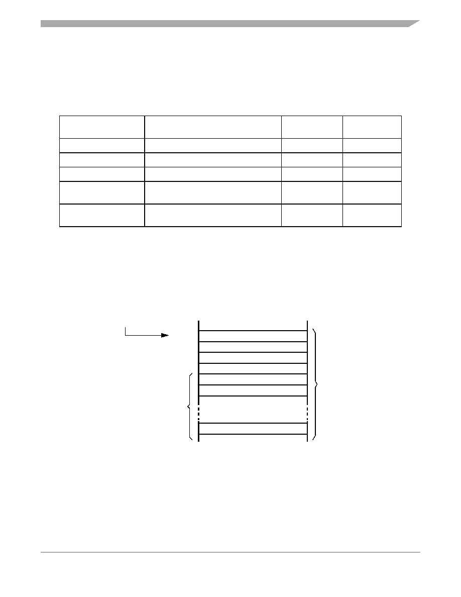
Table 7-10. Summary of ROM-Resident Routines
Routine Name
Routine Description
Call
Address
Stack Used
(bytes)
PRGRNGE
Program a range of locations
$FE10
16
ERARNGE
Erase a page or the entire array
$FE13
10
LDRNGE
Loads data from a range of locations
$FA31
10
MON_PRGRNGE
Program a range of locations in monitor
mode
$FF24
18
MON_ERARNGE
Erase a page or the entire array in monitor
mode
$FF28
12
DATA SIZE (DATASIZE)
START ADDRESS HIGH (ADDRH)
START ADDRESS LOW (ADDRL)
DATA 0
DATA 1
BUS SPEED (BUS_SPD)
FILE_PTR
DATA N
DATA
ARRAY
$XXXX
DATA
BLOCK
ADDRESS AS POINTER
RA
M
相关PDF资料 |
PDF描述 |
|---|---|
| MCK-RKHT-043 | SIP43, IC SOCKET |
| MCK-AHGG-001 | SIP1, IC SOCKET |
| MCK-AHGG-004 | SIP4, IC SOCKET |
| MCK-AHGG-005 | SIP5, IC SOCKET |
| MCK-AHGG-008 | SIP8, IC SOCKET |
相关代理商/技术参数 |
参数描述 |
|---|---|
| MCH-BUTTON-LP4 | 功能描述:MEMORY CARD HEADER RoHS:否 类别:连接器,互连式 >> 存储器 - PC 卡 - 连接器 系列:- 产品目录绘图:67600-8001 标准包装:1 系列:67600 卡类型:安全数字式 - SD 位置数:12(9 + 3) 连接器类型:连接器和弹出器 插入,移除方法:推入式,推出式 弹出器侧:- 安装类型:表面贴装,直角 特点:开关 板上方高度:0.110"(2.80mm) 安装特点:正常,标准 - 顶部 包装:Digi-Reel® 触点表面涂层:金 触点涂层厚度:2µin(0.05µm) 其它名称:WM19017DKR |
| MCHC11F1CFNE2 | 功能描述:8位微控制器 -MCU 8B MCU 1KRAM 512EE RoHS:否 制造商:Silicon Labs 核心:8051 处理器系列:C8051F39x 数据总线宽度:8 bit 最大时钟频率:50 MHz 程序存储器大小:16 KB 数据 RAM 大小:1 KB 片上 ADC:Yes 工作电源电压:1.8 V to 3.6 V 工作温度范围:- 40 C to + 105 C 封装 / 箱体:QFN-20 安装风格:SMD/SMT |
| MCHC11F1CFNE2 | 制造商:Freescale Semiconductor 功能描述:8-Bit Microcontroller IC |
| MCHC11F1CFNE2R | 功能描述:8位微控制器 -MCU 8B MCU 1KRAM 512EE RoHS:否 制造商:Silicon Labs 核心:8051 处理器系列:C8051F39x 数据总线宽度:8 bit 最大时钟频率:50 MHz 程序存储器大小:16 KB 数据 RAM 大小:1 KB 片上 ADC:Yes 工作电源电压:1.8 V to 3.6 V 工作温度范围:- 40 C to + 105 C 封装 / 箱体:QFN-20 安装风格:SMD/SMT |
| MCHC11F1CFNE3 | 功能描述:8位微控制器 -MCU 8B MCU 1KRAM 512EE RoHS:否 制造商:Silicon Labs 核心:8051 处理器系列:C8051F39x 数据总线宽度:8 bit 最大时钟频率:50 MHz 程序存储器大小:16 KB 数据 RAM 大小:1 KB 片上 ADC:Yes 工作电源电压:1.8 V to 3.6 V 工作温度范围:- 40 C to + 105 C 封装 / 箱体:QFN-20 安装风格:SMD/SMT |
发布紧急采购,3分钟左右您将得到回复。