- 您现在的位置:买卖IC网 > PDF目录45313 > MCIMX31LCVKN5C (FREESCALE SEMICONDUCTOR INC) 532 MHz, MICROPROCESSOR, PBGA457 PDF资料下载
参数资料
| 型号: | MCIMX31LCVKN5C |
| 厂商: | FREESCALE SEMICONDUCTOR INC |
| 元件分类: | 微控制器/微处理器 |
| 英文描述: | 532 MHz, MICROPROCESSOR, PBGA457 |
| 封装: | 14 X 14 MM, 0.50 MM PITCH, ROHS COMPLIANT, MAPBGA-457 |
| 文件页数: | 43/122页 |
| 文件大小: | 1418K |
| 代理商: | MCIMX31LCVKN5C |
第1页第2页第3页第4页第5页第6页第7页第8页第9页第10页第11页第12页第13页第14页第15页第16页第17页第18页第19页第20页第21页第22页第23页第24页第25页第26页第27页第28页第29页第30页第31页第32页第33页第34页第35页第36页第37页第38页第39页第40页第41页第42页当前第43页第44页第45页第46页第47页第48页第49页第50页第51页第52页第53页第54页第55页第56页第57页第58页第59页第60页第61页第62页第63页第64页第65页第66页第67页第68页第69页第70页第71页第72页第73页第74页第75页第76页第77页第78页第79页第80页第81页第82页第83页第84页第85页第86页第87页第88页第89页第90页第91页第92页第93页第94页第95页第96页第97页第98页第99页第100页第101页第102页第103页第104页第105页第106页第107页第108页第109页第110页第111页第112页第113页第114页第115页第116页第117页第118页第119页第120页第121页第122页
Electrical Characteristics
MCIMX31/MCIMX31L Technical Data, Rev. 4.1
Freescale Semiconductor
27
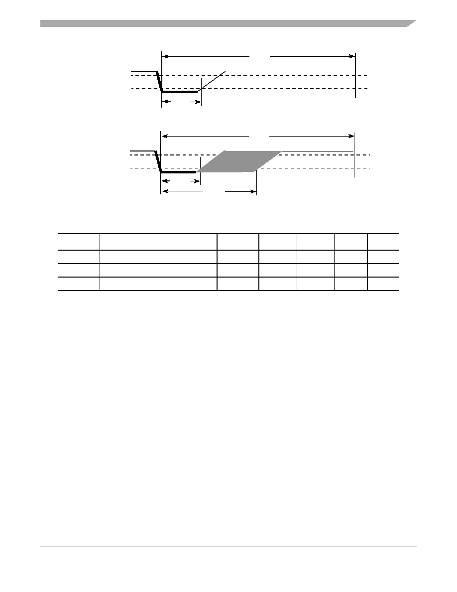
Figure 9. Write 1 Sequence Timing Diagram
Figure 10. Read Sequence Timing Diagram
4.3.5
ATA Electrical Specifications (ATA Bus, Bus Buffers)
This section discusses ATA parameters. For a detailed description, refer to the ATA specification.
The user needs to use level shifters for 3.3 Volt or 5.0 Volt compatibility on the ATA interface.
The use of bus buffers introduces delay on the bus and introduces skew between signal lines. These factors
make it difficult to operate the bus at the highest speed (UDMA-5) when bus buffers are used. If fast
UDMA mode operation is needed, this may not be compatible with bus buffers.
Another area of attention is the slew rate limit imposed by the ATA specification on the ATA bus.
According to this limit, any signal driven on the bus should have a slew rate between 0.4 and 1.2 V/ns with
a 40 pF load. Not many vendors of bus buffers specify slew rate of the outgoing signals.
When bus buffers are used, the ata_data bus buffer is special. This is a bidirectional bus buffer, so a
direction control signal is needed. This direction control signal is ata_buffer_en. When its high, the bus
should drive from host to device. When its low, the bus should drive from device to host. Steering of the
signal is such that contention on the host and device tri-state busses is always avoided.
Table 23. WR1/RD Timing Parameters
ID
Parameter
Symbol
Min
Typ
Max
Units
OW7
Write 1 / Read Low Time
tLOW1
1
5
15
s
OW8
Transmission Time Slot
tSLOT
60
117
120
s
OW9
Release Time
tRELEASE
15
—
45
s
OW7
OW8
1-Wire bus
(BATT_LINE)
OW7
OW8
OW9
1-Wire bus
(BATT_LINE)
Because
of
an
order
from
the
United
States
International
Trade
Commission,
BGA-packaged
product
lines
and
part
numbers
indicated
here
currently
are
not
available
from
Freescale
for
import
or
sale
in
the
United
States
prior
to
September
2010:
i.MX31
Product
Family
相关PDF资料 |
PDF描述 |
|---|---|
| MCIMX31VMN5C | 532 MHz, MICROPROCESSOR, PBGA473 |
| MCIMX31CVKN5C | 532 MHz, MICROPROCESSOR, PBGA457 |
| MCIMX31CVKN5CR2 | 532 MHz, MICROPROCESSOR, PBGA457 |
| MCIMX31VKN5B | 532 MHz, MICROPROCESSOR, PBGA457 |
| MCIMX31LVKN5BR2 | 532 MHz, MICROPROCESSOR, PBGA457 |
相关代理商/技术参数 |
参数描述 |
|---|---|
| MCIMX31LCVKN5CR2 | 功能描述:IC MPU MAP I.MX31L 457-MAPBGA RoHS:是 类别:集成电路 (IC) >> 嵌入式 - 微控制器, 系列:i.MX31 标准包装:1 系列:AVR® ATmega 核心处理器:AVR 芯体尺寸:8-位 速度:16MHz 连通性:I²C,SPI,UART/USART 外围设备:欠压检测/复位,POR,PWM,WDT 输入/输出数:32 程序存储器容量:32KB(16K x 16) 程序存储器类型:闪存 EEPROM 大小:1K x 8 RAM 容量:2K x 8 电压 - 电源 (Vcc/Vdd):2.7 V ~ 5.5 V 数据转换器:A/D 8x10b 振荡器型:内部 工作温度:-40°C ~ 125°C 封装/外壳:44-TQFP 包装:剪切带 (CT) 其它名称:ATMEGA324P-B15AZCT |
| MCIMX31LCVKN5D | 功能描述:处理器 - 专门应用 2.0.1 CONSUMER LITE RoHS:否 制造商:Freescale Semiconductor 类型:Multimedia Applications 核心:ARM Cortex A9 处理器系列:i.MX6 数据总线宽度:32 bit 最大时钟频率:1 GHz 指令/数据缓存: 数据 RAM 大小:128 KB 数据 ROM 大小: 工作电源电压: 最大工作温度:+ 95 C 安装风格:SMD/SMT 封装 / 箱体:MAPBGA-432 |
| MCIMX31LCVKN5DR2 | 功能描述:处理器 - 专门应用 2.0.1 CONSUMER LITE RoHS:否 制造商:Freescale Semiconductor 类型:Multimedia Applications 核心:ARM Cortex A9 处理器系列:i.MX6 数据总线宽度:32 bit 最大时钟频率:1 GHz 指令/数据缓存: 数据 RAM 大小:128 KB 数据 ROM 大小: 工作电源电压: 最大工作温度:+ 95 C 安装风格:SMD/SMT 封装 / 箱体:MAPBGA-432 |
| MCIMX31LCVMN4C | 功能描述:处理器 - 专门应用 TORTOLA MX31 AUTO FULL RoHS:否 制造商:Freescale Semiconductor 类型:Multimedia Applications 核心:ARM Cortex A9 处理器系列:i.MX6 数据总线宽度:32 bit 最大时钟频率:1 GHz 指令/数据缓存: 数据 RAM 大小:128 KB 数据 ROM 大小: 工作电源电压: 最大工作温度:+ 95 C 安装风格:SMD/SMT 封装 / 箱体:MAPBGA-432 |
| MCIMX31LCVMN4CR2 | 功能描述:处理器 - 专门应用 TORTOLA MX31 AUTO FULL RoHS:否 制造商:Freescale Semiconductor 类型:Multimedia Applications 核心:ARM Cortex A9 处理器系列:i.MX6 数据总线宽度:32 bit 最大时钟频率:1 GHz 指令/数据缓存: 数据 RAM 大小:128 KB 数据 ROM 大小: 工作电源电压: 最大工作温度:+ 95 C 安装风格:SMD/SMT 封装 / 箱体:MAPBGA-432 |
发布紧急采购,3分钟左右您将得到回复。