- 您现在的位置:买卖IC网 > PDF目录10934 > MCIMX515DVK8C (Freescale Semiconductor)IC MPU I.MX51 527MABGA PDF资料下载
参数资料
| 型号: | MCIMX515DVK8C |
| 厂商: | Freescale Semiconductor |
| 文件页数: | 124/202页 |
| 文件大小: | 0K |
| 描述: | IC MPU I.MX51 527MABGA |
| 标准包装: | 160 |
| 系列: | i.MX51 |
| 核心处理器: | ARM? Cortex?-A8 |
| 芯体尺寸: | 32-位 |
| 速度: | 800MHz |
| 连通性: | 1 线,EBI/EMI,以太网,I²C,IrDA,MMC,SPI,SSI,UART/USART,USB OTG |
| 外围设备: | DMA,I²S,LCD,POR,PWM,WDT |
| 输入/输出数: | 128 |
| 程序存储器类型: | ROMless |
| RAM 容量: | 128K x 8 |
| 电压 - 电源 (Vcc/Vdd): | 0.8 V ~ 1.15 V |
| 振荡器型: | 外部 |
| 工作温度: | -20°C ~ 85°C |
| 封装/外壳: | 527-LFBGA |
| 包装: | 托盘 |
第1页第2页第3页第4页第5页第6页第7页第8页第9页第10页第11页第12页第13页第14页第15页第16页第17页第18页第19页第20页第21页第22页第23页第24页第25页第26页第27页第28页第29页第30页第31页第32页第33页第34页第35页第36页第37页第38页第39页第40页第41页第42页第43页第44页第45页第46页第47页第48页第49页第50页第51页第52页第53页第54页第55页第56页第57页第58页第59页第60页第61页第62页第63页第64页第65页第66页第67页第68页第69页第70页第71页第72页第73页第74页第75页第76页第77页第78页第79页第80页第81页第82页第83页第84页第85页第86页第87页第88页第89页第90页第91页第92页第93页第94页第95页第96页第97页第98页第99页第100页第101页第102页第103页第104页第105页第106页第107页第108页第109页第110页第111页第112页第113页第114页第115页第116页第117页第118页第119页第120页第121页第122页第123页当前第124页第125页第126页第127页第128页第129页第130页第131页第132页第133页第134页第135页第136页第137页第138页第139页第140页第141页第142页第143页第144页第145页第146页第147页第148页第149页第150页第151页第152页第153页第154页第155页第156页第157页第158页第159页第160页第161页第162页第163页第164页第165页第166页第167页第168页第169页第170页第171页第172页第173页第174页第175页第176页第177页第178页第179页第180页第181页第182页第183页第184页第185页第186页第187页第188页第189页第190页第191页第192页第193页第194页第195页第196页第197页第198页第199页第200页第201页第202页
i.MX51 Applications Processors for Consumer and Industrial Products, Rev. 6
28
Freescale Semiconductor
Electrical Characteristics
The UHVIO type of I/O cells have to be configured properly according to their supply voltage level, in
order to prevent permanent damage to them and in order to not degrade their timing performance.
The HVE control bit of the I/O cell (in IOMUX control registers) should be set to 1 for Low voltage
operation and to 0 for High voltage operation.
The HVE bit should be set as follows:
HVE = 0: High output voltage mode (3.0V to 3.6V)
HVE = 1: Low output voltage mode (1.65V to 3.1V)
This is related to power domains, such as NVCC_NANDF, NVCC_PER15, and NVCC_PER17.
If HVE bit is not set properly when high voltage level is applied for long durations, it may cause permanent
damage over a period of time, causing reduced timing performance of the pad. Similarly, not setting HVE
bit properly for low voltage will degrade pad timing performance.
The below discussion clarifies concerns about boot-up period.
The HVE bit is set, by default, to 1 for low voltage operation. As a result, there might be a short period
conflict between the HVE bit value and the applied voltage. This conflict is acceptable under the following
conditions:
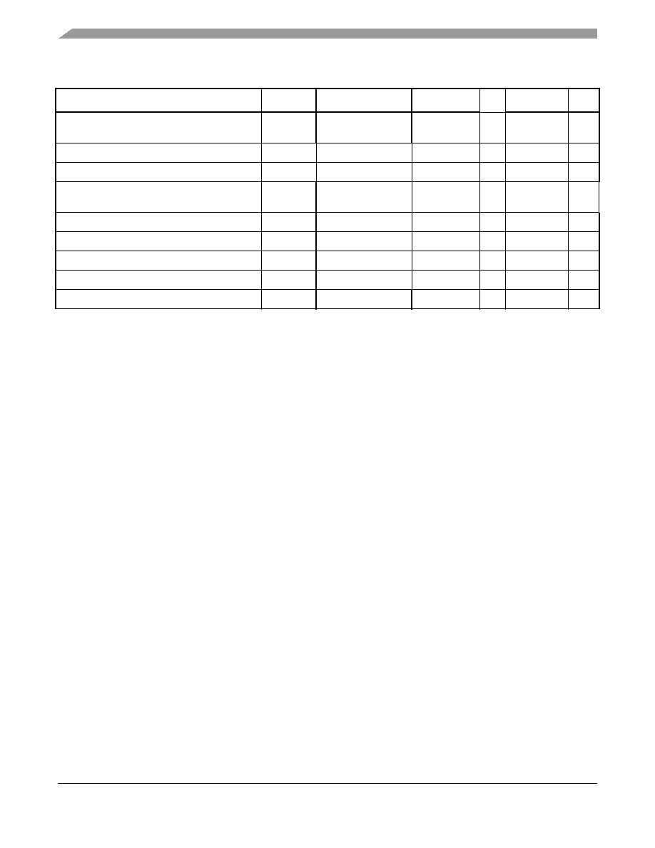
Input Hysteresis
VHYS
Low voltage mode
High voltage mode
0.38
0.95
—0.43
1.33
V
Schmitt trigger VT+2,3
VT+
—
0.5OVDD
—
V
Schmitt trigger VT–2,4
VT–
—
0.5
× OVDD
V
Input current (no pull-up/down)
Iin
Vin = 0
Vin = OVDD
—
See Note 4
—
Input current (22 k
Ω Pull-up)
Iin
Vin = 0
—
202
μA
Input current (75 k
Ω Pull-up)
Iin
Vin = 0
—
61
μA
Input current (100 k
Ω Pull-up)
Iin
Vin = 0
—
47
μA
Input current (360 k
Ω Pull-down)
Iin
Vin = OVDD
—
5.7
μA
Keeper Circuit Resistance
—
NA
—
17
—
k
Ω
1
To maintain a valid level, the transitioning edge of the input must sustain a constant slew rate (monotonic) from the current DC
level through to the target DC level, VIL or VIH. Monotonic input transition time is from 0.1 ns to 1 s.
2 Overshoot and undershoot conditions (transitions above OVDD and below OVSS) on switching pads must be held below 0.6 V,
and the duration of the overshoot/undershoot must not exceed 10% of the system clock cycle. Overshoot/undershoot must be
controlled through printed circuit board layout, transmission line impedance matching, signal line termination, or other methods.
Non-compliance to this specification may affect device reliability or cause permanent damage to the device.
3 Hysteresis of 250 mV is guaranteed over all operating conditions when hysteresis is enabled.
4 I/O leakage currents are listed in Table 25.
Table 21. UHVIO DC Electrical Characteristics (continued)
DC Electrical Characteristics
Symbol
Test Conditions
Min
Typ
Max
Unit
相关PDF资料 |
PDF描述 |
|---|---|
| IDT821024PP | IC PCM CODEC QUAD NONPROG 44TQFP |
| VE-26B-CU | CONVERTER MOD DC/DC 95V 200W |
| MCIMX515DJM8CR2 | IC MPU I.MX51 529MABGA |
| IDT821024JG | IC PCM CODEC QUAD NONPROG 32PLCC |
| VE-263-CU | CONVERTER MOD DC/DC 24V 200W |
相关代理商/技术参数 |
参数描述 |
|---|---|
| MCIMX515DVM8B | 制造商:Freescale Semiconductor 功能描述:APPLICATIONS PROCESSOR TRAY - Bulk |
| MCIMX516AJM6C | 功能描述:处理器 - 专门应用 ELVIS 3.0 RoHS:否 制造商:Freescale Semiconductor 类型:Multimedia Applications 核心:ARM Cortex A9 处理器系列:i.MX6 数据总线宽度:32 bit 最大时钟频率:1 GHz 指令/数据缓存: 数据 RAM 大小:128 KB 数据 ROM 大小: 工作电源电压: 最大工作温度:+ 95 C 安装风格:SMD/SMT 封装 / 箱体:MAPBGA-432 |
| MCIMX516AJM6CR2 | 制造商:Freescale Semiconductor 功能描述:ELVIS 3.0 AUTO NO MV - Tape and Reel |
| MCIMX518DVK8C | 制造商:Freescale Semiconductor 功能描述:ELVIS 3.0 - Bulk |
| MCIMX51EVK | 制造商:Freescale Semiconductor 功能描述: |
发布紧急采购,3分钟左右您将得到回复。